The Japanese Ministry of Economy, Trade and Industry (METI) released September’s production data for the electronics industry in Japan. A nine-month snapshot for the first three quarters is now available, and allows us to review a few market trends and assess our plans for the remainder of the year.
Read more: Q3 Performance of the Japanese PWB Industry
Design considerations for moving from 0.5mm pitch to 0.4mm pitch and below.
Package-on-package is a method of stacking components atop one another. Some OEMs use PoP to reduce the board real estate area, particularly for small handheld products and devices. Others are moving to PoP because end-markets demand greater performance in smaller systems and products. In either case, OEMs will find that there’s a game changer going from 0.5mm pitch BGA PoP to the next generation, 0.4mm ultra-fine pitch BGA PoP.
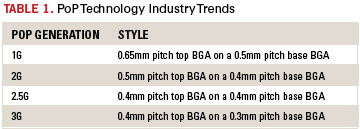
Industry trends say that PoP-populated PCBs will evolve in three stages as shown in Table 1.
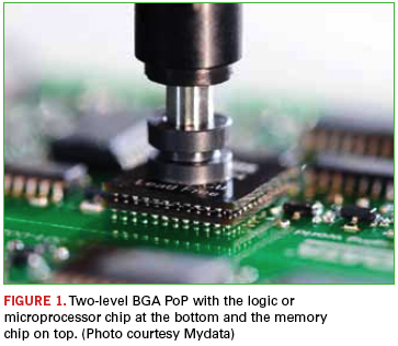
Currently, in some camps, PCB designers are at the first stage using two-level BGA PoP with the logic or µP (processor) chip at the bottom and the memory chip on top (Figure 1). However, there are certain key steps involved in increasing success at the third level. But first, before stepping out with 0.4mm pitch BGA PoP-based PCB designs, it’s important to revisit those rules-of-thumb at the 0.5mm level and above. These rules-of-thumb relate to pad sizes and solder mask openings up to 0.5mm pitch.
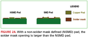
First is to maintain pad size around 85% of the ball size of the BGA. Second is to provide a non-solder mask defined (NSMD) pad whereby the solder mask opening is larger than the NSMD pad (Figure 2a). Typically solder mask is opened to a diameter of around the ball size of the BGA. In this instance, the solder mask is recessed, permitting it to provide stress relief to the NSMD pad during reflow. In short, it creates a protective dam so that solder can go around it.
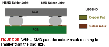
Further, since there are no existing published design guidelines for 0.4mm pitch PoP-based PCBs, be wary of today’s conflicting reports. Issues stemming from these reports deal in large part on PCB pad sizes and solder mask openings. Take, for example, a 0.4mm pitch BGA PCB design using NSMD pad sizes, where in a low-volume run the results were highly acceptable. However, for larger production, this approach produced low yields. By adopting the solder mask defined (SMD) pad approach (Figure 2b), whereby the solder mask opening is smaller than the pad size, better yields and results are achieved. Also, it’s important to note when deploying NSMD pads for 0.4mm and 0.3mm pitch BGA/PoPs, the chances are great of creating bridging between pads due to insufficient solder mask webbing between pads.
Key Factors to Pursue
Since 0.4mm pitch BGA PoP-based PCB design is in its infancy, it is a good idea for the PCB designer to perform preliminary experimental layouts and prototype rounds to get the lay of the design before launching into a full-fledged layout. Rules followed for 0.5mm pitches may not work for 0.4mm cases at high volumes. Typically, ball sizes of 0.4mm pitches are smaller. Reducing the pad size by another 15% may make the solderable area insufficient. Second, using NSMD with 0.4mm parts may cause bridging between adjacent pads. Third, since the pad sizes are so small, and there is no solder mask webbing to provide adhesive strength, it may peel off during reflow or in the field.
Against this backdrop, there are six key factors affecting the reliability of a 0.4mm ultra-fine pitch BGA/PoP-based PCB design. Those are pad design, via-in-pad guidelines, via finish, stencil design, solder paste, and thermal profile.
As suggested, SMD is the pad of choice for 0.4mm pitch. In this case, the pad is created as the same size of the BGA ball. Solder mask opening is around 15% less than the ball diameter. Here, the solder mask laps over the edge of the copper pad to strengthen the connection in a couple ways: One, it strengthens the bonding between the copper and the PCB’s laminate; two, with the copper pad going farther into the solder mask, copper area is larger. That larger copper area provides a greater surface for the PCB laminate to adhere, making the connection twice as strong.
Also, in these designs, traditional BGA dogbone fan out used for larger pitches with extended real estate is not considered at all. Instead, via-in-pad is used, a specialized technique for escape routing fine-pitch BGAs. Before discussing guidelines for use, it’s a good idea to revisit the via-in-pad approach. This escape routing technique involves vias being placed directly on the BGA pads and filled with a conductive or a nonconductive material, which provides a fairly flat surface. Traditionally, silver was used to fill the vias, and a small increase in density was realized so that the designer could route a few more signals on the outer surface. That technique has evolved considerably, and now the materials of choice fall in the nonconductive category. The reason: Vias filled with a nonconductive epoxy perform better because the coefficient of thermal expansion (CTE) is comparable with that of the PCB.
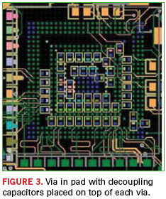
Therefore, the rate of expansion is similar to the board material, allowing for a more reliable joint. Issues like via out gassing and solder voids can be avoided. The same method of filling vias is used on 0.4mm PoP designs. A key point to make is that whenever there are vias below a BGA and available for connection, they should be filled, tented, or capped. Otherwise, they can cause voids and out-gassing during reflow. Also, as shown in Figure 3, discrete decoupling capacitors can be placed directly over the vias on the bottom side. This provides a low inductance path to the power system.
Place and Route
When it comes to 0.4mm pitch BGA PoP, it’s not a good idea to place a BGA on the opposite side of another BGA, which is the typical case in 0.5mm pitch BGA and above. Instead, BGA/PoPs should be placed offset from each other with about 500 mils spacing to maintain board level reliability and ease of debugging on the bench when needed.
Again, since 0.4mm pitch BGA/PoPs are so new, manual routing is recommended over autorouting. Reason: An autorouter is a computer program based on mathematical algorithms and fixated on making connections. It doesn’t think like a human designer. In most instances, using the autorouter results in unusual traces, many unnecessary vias routed and many unnecessary loops.
In effect, the autorouter creates more vias than are required, thus reducing the reliability of the final assembly. Also, those extra vias add discontinuities if the design calls for certain impedance requirements. Typically, impedance is based on the geometry of the connection from driver to receiver. Hence, that impedance path needs to be uniform. Whenever there is a via, there is a discontinuity in that uniform pad, and impedance changes at that particular moment. Ideally, for a 0.4mm pitch BGA/PoP-based design with high-speed signals, you don’t want a via. Additional vias will cause considerable discontinuities and subsequent ringing and reflections.
While performing the routing, it’s also vital to avoid creating heat sinks. How can a designer inadvertently do this? This occurs when a trace is put on a via or a dogbone fan out is performed from a via that’s almost the same size as the pad. The result is the traces and vias pull heat away from the BGA/PoP and cause issues during assembly. In another example, copper pour is placed over BGAs. This may happen when there are multiple power/ground pins on the device. During assembly, this arrangement will sink the heat during reflow and cause cold solder joints, resulting in opens or intermittent connections.
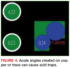
Also, in the realm of routing, acute angle traces should be avoided when connecting BGA pads, as they could result in acid traps. Acid traps are acute angle areas or small areas where etching chemicals get stuck, and eventually, those small chemicals eat away the traces and intermittent connections result (Figure 4). Finally, the designer should design with metric units rather than English for fine-pitch BGA devices and PoP. This will not only increase accuracy, but will also avoid requiring four decimal places of accuracy when converting from micrometers to mils.
Team Effort
There’s always talk about working together to successfully complete a project. But in the case of 0.4mm ultra-fine pitch BGA/PoP-based PCBs, there is no question it is essential that the PCB designer, fabricator and assembler work in unison, with the designer taking the lead. The PCB designer must maintain regular discussions with the fabricator to understand its capabilities, such as determining whether it can handle certain minimum hole size aspect ratios. Part of that dialogue includes understanding the spacings for a high-speed design’s impedance control traces, and knowing the chosen substrate material’s capacity to handle those requirements. Furthermore, the designer must have a good handle on a fabricator’s manufacturing limits. Those can be divided into three categories: standard technology, high-yield, and engineering development. The first refers to a fabricator’s capability, for example, 5 mil traces and spacing, which is a midrange capability for most board shops today. For mass production, high yield is typically 8 mil lines and spaces. (These numbers are relative, so for some fabricators, 10 mils will be high yield, while 8 mils might be typical for others.) Third, there’s the engineering development category. This deals with a fabricator’s highly advanced capabilities, which fall into the 2.5 mil traces and 2.5 mil spacing class.
The layout designer must also know the assembler’s capabilities, such as the minimum pitch that assembler can work with. Either it can or cannot perform 0.4mm ultra-fine pitch BGA/PoP PCB assembly. If it is building 0.4mm pitch, what kind of solder paste are they using? Are they following manufacturer’s recommendations on the reflow profile? The designer must also have discussions with the paste manufacturer to ensure the right pad sizes are associated with the right solder paste. Avoiding warpage is another key area demanding close interaction between the designer and assembly. By not paying special attention in this area, excessive warpage can result in bridging, solder slumping, head in pillow, or opens.
PoP is an emerging technology, and will be utilized more as the industry gears toward further miniaturization of the existing technologies. Do not assume that the same techniques that work for larger versions will necessarily scale to the smaller ones.
IPC’s new president has put the attention back where it belongs: on member needs.
Want to know how new IPC president John Mitchell is? He still calls members “customers.” It’s, as they say in Las Vegas, a “tell,” a verbal tic that gives away what someone is thinking.
In this case, that’s a good thing. When we met with Mitchell in the IPC offices in Bannockburn, IL, on Aug. 9, he wasn’t quite four months officially into the new job. But over the course of our conversation, the former Bose and Alpine Electronics executive quickly showed where his head is at, stressing repeatedly that the 55-year-old association needs to refocus on its members.
At that point, Mitchell had spent much of his first few weeks visiting OEMs, fabricators and EMS companies, asking again and again, “What are your big challenges?” Most ticked off two to seven items each, for an aggregate 35 issues, of which 30, he said, IPC has some effect on. That list now becomes the battery for the IPC engine. “Where we put our effort is where we can help,” he says.
IPC has come under criticism from many quarters over its insular nature and brusque relations with other organizations and even some members. Mitchell, who comes across as highly detailed and involved, did not shy away from that discussion. In fact, he capitalized on it. Recognizing the IPC culture needed to reposition from how to grow IPC to how to help the members, Mitchell has restructured the organization to better underscore the notion of IPC staff member as account representative. “We help IPC members realize the benefits IPC can give them. We need to be local in feel.”
Not that every program needs an overhaul. Mitchell noted the strengths of the technical programs and trade shows as two areas that are functioning properly. “IPC has done some pretty good things. We have some good basic stuff. The standards provide commonality across the globe.”
Likewise, the Apex Expo exhibition is a “great thing”, he says, although improvements are always possible. Mitchell, who has two decades’ experience in consumer electronics, noted that the CES attracts the entire chain from designers to supplier to customer. “It’s a massive meeting of the industry, where we can accomplish a great deal.” He wants Apex Expo to accomplish that same lofty goal, suggesting daily “themes,” such as medical, automotive and consumer to appeal to a wider audience.
One area IPC has encountered challenges is in meeting the demands of a wide variety of constituents, some of whose needs are in conflict. Mitchell is quick to acknowledge addressing those tensions won’t be simple. “There are different benefits IPC needs to provide to different-sized organizations. We need to be flexible enough and listen to the members to do this well. For the smallest companies, I don’t know the best way to help them yet, but we will figure it out.
“I have to provide 10 times the value, 100 times the value, whatever it is. That’s how we’ll determine what we should be doing. Does it add value to our members? It shouldn’t be only for the benefit of IPC. It’s all about providing member value.”
An engineer by education and training, he is optimistic, however, about how the technology can both bring members together and present an unbounded future. “Printed electronics is an awesome opportunity for growth in the US. The industry can get together with graphics manufacturers and raise their expertise and find new markets. Our job is to transfer technology and information on the importance of that technology.”
Other opportunities, he adds, for IPC to help its members include market research and government relations. “It’s not just about only doing things for the future, it’s about helping the current business situation. We look at how to close the gap.”
Our conversation turned to working with other associations, something IPC has occasionally struggled with. Mitchell said, “Associations don’t have to function like businesses and be competitive with each other. There are huge collaboration opportunities.” Interestingly enough, two months later, he agreed to move IPC’s semiannual task group meetings to SMTAI, a move that will firm up support of the latter event, while saving time and money for countless IPC members.
Government relations are another complicated area. IPC’s membership is worldwide, and many MNCs either have their own lobbyists or are reluctant to support efforts that might hamper their competitiveness outside the US, facts Mitchell readily acknowledges. “It’s largely about the medium and smaller organizations. GR is tricky for IPC. We can’t say, ‘We will fight an issue that will only help US manufacturers.’ But global issues, we can go after these. Conflict minerals – even though that is US-focused, the MNCs want to build one product that is used everywhere. We mobilize when we can bring science to the issue.”
Mitchell’s enthusiasm and thoughtfulness make him the right person to lead IPC, and he’s ready for the challenge. “We’ve got a good foundation. We are in a very stable position. Here, we have opportunities to serve our members.”
A unified front might be the trick to obtaining a fair price.
While it could be said that our industry, steeped in a tradition of phenomenal technological breakthroughs, has done some really fantastic things over the years, one thing that we have collectively failed miserably at is conveying the value that the design, fabrication and assembly of printed circuit boards provides the end-user. Worse, I question whether we even know how to measure the true cost of the value we bring to our collective customer base.
What is “value?” I view value – total value – as the sum of all parts that go into providing a product. The sum of all the parts includes not only the materials and supplies that make up a product, but also the competent and innovative people, regardless of academic background, who actually make it, and the investment in the best available equipment – which does not necessarily mean the newest. Equally, the sum of the parts includes the oft-forgotten but essential “little things,” like commitment to adequate inventory, training staff on new processes and methods, and servicing customers that all too often need considerable hand-holding to understand the options available to get what they are ultimately asking for – all with exceptional quality, delivered quickly and on-time.
Collectively, we have been mediocre at best at explaining (read: selling) this value. Trade groups have failed to broach head-on a meaningful discussion of the value our industry collectively provides to end-customers. Ditto for the supply base. Worst of all, the individual companies aggressively tout their abilities but don’t connect the dots in terms of how their products and services really benefit end-customers. Rather than marketing the value that goes into the design and manufacture of PCBs, each company will discuss in vague generalities why they are better than the others, or how they can save the end-customer some money on the next order. Rarely do any of us tell customers that collectively we all provide significant value, and therefore, with all due respect Mr. Customer, we all should be valued!
Why tell a customer that everyone – not just your specific company – is of value? Because only by selling the value of all companies will any company be able to command what they are worth in the marketplace. Customers hear only the bean-counter mantra that we all are just commodities. Instead, customers need to hear that, regardless of our location, niche or size, we are all providing true value, are worth the price we charge, and perhaps they, the customer, should pay more attention as to whom they buy from, and why.
This is not about fixing prices or other collusion but rather presenting a unified front to promote what we all apparently take for granted: that there is real value to what we do. We as an industry – associations, suppliers and manufacturers – owe it to ourselves and each other to educate customers on that value, and that value needs to be reflected in a fair price.
A fair price also requires understanding, valuing and charging based on the accurate cost of product development and manufacture. Rather than incorporating the total cost into a price, we fall victim to competition, real or perceived. How often do we complain about the renegade “bucket shop” or “big company from wherever” that drops its price so “none of us” can make money? Maybe instead we should remind customers that those who drop prices just to fill their plant have more often than not failed, leaving customers stuck with no product.
Possibly a better approach would be to add to our sales presentations the value our products and services provide, and explain the total cost that goes into each job processed and manufactured. Equally, maybe in little ways we can all, together, reinforce that true value is being provided, and not capitulate when customers demand unrealistic price targets or extended payment terms “like the distributors accept.” None of us are distributors; we build to print and purchase specific materials processed per specification and, therefore, have total costs that go into providing true value. If everyone holds their end up, the message will get across! This is not for the faint of heart. Make no mistake, customers love when an industry works together, by plan or by accident, to create a downdraft in pricing. In fact, customers encourage this by convincing suppliers that what they provide is of little or no value. And when this happens, regrettably too often we as an industry capitulate. Yes, some may resist, but a chain is only as strong as its weakest link. If one firm breaks ranks, we all suffer.
Long-term, to remain viable, we need to do a better job conveying how much value we all, together, provide customers. This requires a multifaceted approach. Yes, we need to continue to explain our technology and service. However, we have to expand on that to include the true cost of providing ever-improving service and investing in cutting-edge technologies. Equally, we need to better communicate the outstanding technical competence required of employees throughout the industry. Circuit boards and all they go into are not designed, fabricated or assembled strictly by machines. Skilled people make it happen, and that is a core value – and true cost – too often ignored or undervalued by end-customers, and rarely effectively communicated by our industry as a differentiator.
Our industry has a tradition of being innovative. Clearly our companies have excelled as technology leaders. Isn’t it time that, together, we fashion a message that all the companies that provide the leading edge technology that end-users have come to expect are providing true value?
Consolidation has been occurring for years in the electronics supply chain, and distributors have been no strangers to the phenomenon. In fact, just over a month ago we interviewed David Wolff, founder and president of P.D. Circuits, a major US-based bare board broker that was being acquired by NCAB Group of Sweden.
So when the news broke on Sept. 26 at PCB West that P.D.’s main US competitor, Bare Board Group, was putting together a deal of its own, it seemed part of the normal fare.
But when it was revealed just whom BBG was buying, the picture became a lot more interesting.
BBG’s acquisition target was Hunter Technology’s printed circuit board fabrication operations. The move dramatically changes the distribution landscape because, for the first time in years, a major regional distributor will also have internal manufacturing capability.
Although rare these days, the manufacturer-distributor model isn’t a completely foreign concept, but it’s more commonplace among contract electronics assemblers. No fewer than five firms in the CIRCUITS ASSEMBLYDirectory of EMS Companies offer some degree of component or equipment reselling. Most are small. Jaco Electronics in New York offers name-brand flat-panel displays, but also performs some degree of CTO box-build and assembly. T-Tech Electronics in Penang distributes components and offers EMS services. STI in Huntsville, AL, is a Tier IV EMS and reps various equipment lines. In January, electronic components manufacturer AirBorn acquired EMS firm AESCO Electronics.
Others have tried on a larger scale and failed. After acquiring contract assembler Hibbing Electronics in 1998, components disty Reptron’s sales quickly peaked, topping $300 million. Within five years came a reorganization. After two more years of repeated losses, it was sold to Kimball. In 2005, when EMS firm Rad Technologies acquired a distribution operation, it had the goal of reaching $100 million in annual sales within the year. It, too, is now out of business. Even fewer component distributors have attempted to broker bare boards. When we researched the market a few years ago, we found only one company – Elfa, in Sweden – offering PCBs on its line card. More typical is an arrangement whereby a disty links its website to that of a fabricator’s, thus simplifying the board buying process. A year ago, for instance, element14 did just that through partnerships with PCB manufacturers Sunstone Circuits and Pentalogix.
A few months back, PCB distributor Fineline Global announced a 25% stake in Shenzhen Fastprint Circuit Tech. What’s less clear, however, is whether Fineline is doing more than simply investing in the fabricator.
That’s why BBG’s move represents a more significant undertaking. Distributors have traditionally shied away from product build because the two models require different sets of business practices. Inventory turns are valued in both industries, of course, but outsourced manufacturing emphasizes service over commoditization. PCBs are not off-the-shelf parts; each part number is a unique design. And then there’s the conundrum of how the disty keeps its other circuit board suppliers happy, while also maintaining its own loaded factory. BBG is novel in trying to cross that bridge.
But there’s a tempting potential payoff. PCB distributors are now pushing into the $100 million realm, which would be big enough to make Dr. Hayao Nakahara’s NTI-100 list of the largest board fabricators (which we published in September). NCAB’s acquisition of P.D. puts it up against that magic revenue number.
The Hunter deal won’t get BBG there, not by a long shot. Privately held Hunter doesn’t report revenues from its fab operations, but they likely aren’t higher than $4 million a year. BBG’s annual run rate is about $30 million.
Still, as BBG founder and president Greg Papandrew told me years ago, the one disadvantage he always faced selling against bricks-and-mortar board shops was not having what he called the “storefront.” Apple sold lots of iPhones and iPods through the traditional channel, but things really took off when it opened its own retail stores. Sometimes, customers just want to feel close to the original supplier.
To be sure, almost every US- or Europe-based fabricator also brokers boards. IPC data indicate close to one-fifth of the boards sold in the US by domestic fabricators were purchased from offshore sources. So BBG will be up against not only the dedicated disty competitors, but also an army of small shops – most roughly the size of Hunter – which already have overseas partners.
In the end, the model itself is less important than the execution. If BBG, or others that follow in its footsteps, can continue to get reliable PCBs into the hands of customers on-time and on-budget, this will look like a brilliant move. And if not, it won’t.
Abstract: In this study, an accelerated test condition [130°C, 85% RH, and 100V DC] was used to investigate conductive anodic filament (CAF) in two organic package substrates: 1) cyclo-olefin polymer–glass fiber composite (XR3) and 2) epoxy-glass fiber composite (FR-4). Test coupons with through-via spacing of 100µm and 200µm were investigated. CAF failures were not observed in either substrate type with spacing of 200µm. With spacing of 100µm, insulation failures were observed in FR-4, while XR3 exhibited stable insulation resistance during the test. The substrates were characterized using gravimetric measurement, and XR3 was found to exhibit significantly lower moisture absorption compared with FR-4. CAF failures in FR-4 were characterized using scanning electron microscopy and energy-dispersive x-ray spectroscopy. Results suggest a strong effect of moisture sorption of organic resins on CAF failure at smaller through-via spacing in package substrates. (Journal of Electronics Materials, November 2012)
PCB Substrates
“Data Mining for Creep Corrosion on Desktop Computers”
Abstract: When the PC industry switched from traditional leaded (SnPb) solders to lead-free (SnAgCu) solders, the industry considered new board surface finishes as well. The corrosion resistance of the leading Pb-free coatings, immersion silver (ImAg) and organic solder protectant (OSP) were questioned. With several years of field experience, organizations can quantify the efficacy of ImAg and OSP with actual field data. For the past few years, Intel’s warranty return centers performed a visual inspection for corrosion on all motherboards returned. A statistical analysis was performed on all returned products to determine the general extent of corrosion and to look for subpopulations with statistically significantly higher and lower return rates. It was found that excessive flux application dramatically affected the corrosion incident rate for motherboard products with ImAg finishes. No correlation existed between the percentage of sales to particular countries or geographies and the relative corrosion incident rates for the desktop motherboard part numbers in the study. Newer motherboard part numbers with OSP coatings experienced significantly reduced incidents of corrosion compared to earlier motherboards with ImAg coatings. Components on desktop motherboards showed no obvious signs of creep corrosion in the warranty returns population studied. (SMTA International, October 2012)
Solder Joint Reliability
“Characterization of Stress–Strain Response of Lead-Free Solder Joints Using a Digital Image Correlation Technique and Finite-Element Modeling”
Authors: G. Khatibi, M. Lederer, E. Byrne, A. Betzwar Kotas, B. Weiss and H. Ipser
Abstract: The stress-strain response of miniaturized Sn-Ag-Cu (SAC) lead-free solder joints in the thickness range of 80µm to about 1.1mm was studied. A high-resolution 3D digital image correlation system was used for in situ measurement of displacement and strain fields in the solder joints during tensile testing. These measurements showed that the localization of plastic strain and stress buildup occurs mainly at the interface of the solder. With increasing solder gap thickness, the size of the plastically deformed zone in the solder increases, resulting in transformation of a brittle interfacial fracture to a ductile fracture within the bulk of the solder. The experimental deformation plots of solder joints and strain-rate-dependent tensile tests on bulk solder material were used to establish a new constitutive material model for the solder. This strain-rate- and pressure-dependent material model was implemented in ABAQUS through the user subroutine CREEP. In agreement with the experiments, the finite-element method simulation revealed a pronounced thickness effect leading to higher tensile strength of thinner solder joints. (Journal of Electronics Materials, November 2012)
“Reliability of Passive and Active Components with Differences According to Lead-Free Paste Characterization”
Abstract: Components were analyzed according to shear stress and solder joint cracking. The study compared different flux and solder paste formulations in terms of wetting properties, void formation and reliability results for active and passive components. For passive components, pure nickel and tin finishes were compared. Shear stress was analyzed under automotive requirements. Test conditions used in the testing procedure were temperature cycling with different parameters in terms of deltaT: -40°/+125°C (30'/10"/30'). Data are available for 2000 cycles. Active components were also tested with this procedure. These components had different finish terminations, such as tin and NiPdAu/Ag for LQFPs, and eutectic SnAg and SAC balls for BGAs. Analysis was performed by cross-section and crack length after cycling measured. (SMTA International, October 2012)
This column provides abstracts from recent industry conferences and company white papers. Our goal is to provide an added opportunity for readers to keep abreast of technology and business trends.