Underfilms have material properties similar to underfills but are easier to process.
A common failure mode for portable electronics is mechanical failure as a result of being dropped from sufficient height to cause damage. Most portable electronics producers qualify assemblies by performing some type of system-level drop test, while component suppliers typically utilize industry standard drop tests such as JEDEC JESD22-B111.1 It is well known that Pb-free solders do not perform as well in drop or shock testing as the Pb-free solders they replaced.
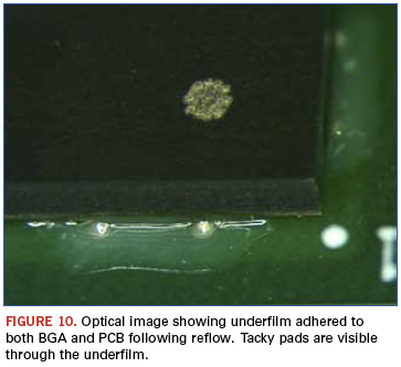
Much work has been carried out to optimize Pb-free alloys to improve drop test performance.2-6 Many companies have also implemented epoxy underfill to further increase robustness of the interconnection between the BGA and printed circuit board. These underfills are typically dispensed around the BGA following SMT assembly and electrical testing. Capillary action then slowly draws the underfill under the BGA. The underfill may be dispensed in sufficient volume to cover the entire BGA underside, the corner areas only or just the package sides. Finally, the underfill is cured in an offline batch oven. While excellent drop test results have been demonstrated with underfill, the process adds cycle time and may involve processes not normally performed during assembly. Another option for providing greater BGA to PCB mechanical robustness that may provide a more seamless integration into the SMT manufacturing process is the use of a preform underfilm material.7 The material can typically be provided in reels similar to discretes and is placed around the perimeter of the BGA following solder paste printing and prior to BGA placement. In reflow, the underfilm softens and initially expands such that it contacts both the BGA and the PCB. By the conclusion of reflow, the material fully cures, while remaining adhered to both the BGA and PCB.
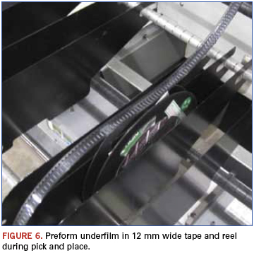
For our study, the preform underfilm material was a fully cured, low flow polyurethane polymer. It comes in a variety of shapes and sizes, and for this study it was specified in 4.0 x 0.76mm preforms with a thickness of 0.165mm. The preforms were provided in EIA-481-compatible 12mm wide carrier tape with a cover tape similar to how discretes would be supplied. The underfilm material is a thermoplastic designed to soften, flow and expand during reflow, thereby filling in the gap between package and PCB. Upon cooling in the reflow oven, the material resolidifies and bonds the package to the PCB. For this study, it was decided to use two of the preforms per corner, which effectively formed an L-shaped pattern. It should be noted that L-shaped preforms could also have been used.
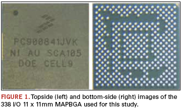
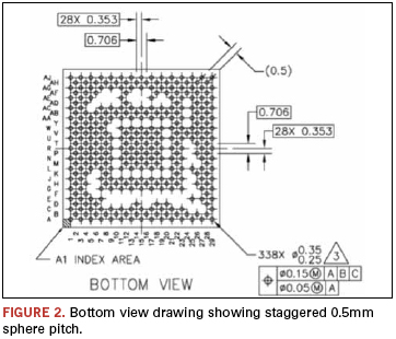
The test vehicle (Figure 1) was a 338 sphere 11 x 11mm body size PBGA with spheres at a staggered 0.5mm pitch (Figure 2). It is a package typical of portable electronics applications. The composition of the Pb-free spheres was SAC 105 (98.5%Sn, 1.0%Ag, 0.5%Cu by weight). The PBGA was molded all the way to the substrate edge in what is called a Mold Array Process (MAP).
The dummy die size inside the daisy-chain package was 5.3 x 5.4 x 0.28mm; the two-layer substrate thickness was 0.21mm, and the total package thickness excluding spheres was 0.92mm. The pads on the package were SMD with a specified 0.38mm copper diameter and a 0.30mm soldermask opening.
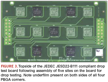
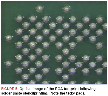
The test board used was based on the JEDEC drop testing specification for devices with less than or equal to a 15 x 15mm body size. The board (Figure 3) was 132 x 77mm and 1.0mm thick with eight layers of copper. The surface finish was OSP. SMD pads on the PCB were designed to exactly match the package, with a copper diameter of 0.38mm and a soldermask diameter of 0.30mm. The only modification made to the test board to accommodate the underfilm preforms was the addition of four additional pads in each corner of the package footprint. Once printed with solder paste, these tacky pads served as a way to keep the underfilm in place prior to reflow.
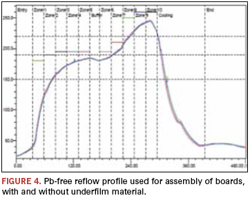
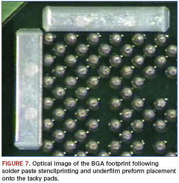
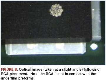
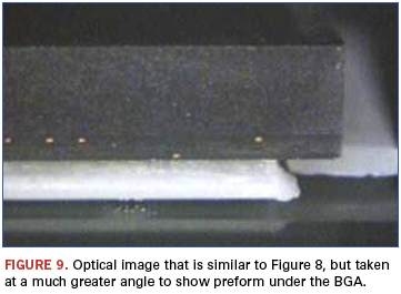
Assembly was carried out using a high-volume production SMT line with automated pick-and-place equipment and automated solder paste volume inspection. PBGAs were supplied in JEDEC trays. The Pb-free solder paste used was a halogen-free, no-clean with a SAC 305 composition (96.5%Sn, 3.0%Ag, 0.5%Cu). The reflow profile (Figure 4) had a peak temperature of 244.5º to 246ºC, depending on thermocouple location. Total reflow time was approximately six minutes. Each underfilm preform was placed on the two tacky pads near each corner of the part following solder paste printing. BGAs were then placed normally. Figures 5 to 10 show photos taken at various steps in the assembly process from printing and underfilm preform placement through BGA placement and reflow.
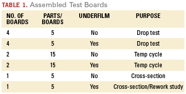
As shown in Table 1, a total of 14 boards containing 130 total components were assembled. On the boards for drop test, only five sites were populated (Figure 3). This is permitted by the JEDEC standard and was done to provide the most consistent drop test results by not populating parts close to corner standoffs. For the boards for thermal cycling, all 15 sites were assembled. Two additional boards were assembled for cross-sectioning. One hundred percent yield was achieved in assembly, and all underfilmed BGAs appeared to have the material adhered as expected between the BGA and the PCB in all four corners.
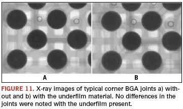
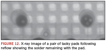
X-ray analysis. Following assembly, all boards underwent x-ray, with close attention paid to corner joints that may be in contact with the underfilm material. No misshapen or anomalous solder joints, such as those with opens, shorts, or excessive voiding, were observed (Figure 11). Additionally, the tacky pad locations were x-rayed, and all the printed solder paste was seen to be soldered to the pad, as opposed to being dispersed in the underfilm (Figure 12).
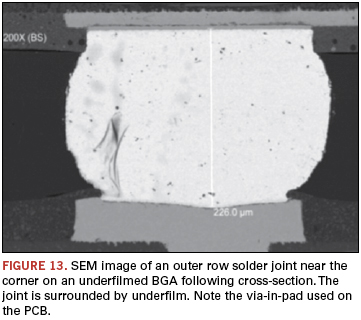
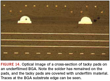
Cross-sectional analysis. Underfilmed and non-underfilmed BGAs were both cross-sectioned to the outer row to assess the solder joint formation and standoff (Figure 13). The underfilm was seen to be enveloping the three to four solder joints closest to the corner. The solder joint standoff between the underfilmed and non-underfilmed BGAs was found to be similar. A cross-section through the tacky pads on an underfilmed sample further confirmed that the solder paste reflowed and remained on the tacky pads (Figure 14).
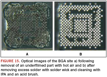
Underfilm rework evaluation. Using an extra board that was assembled with underfilm, a small study was carried out to ascertain the reworkability of underfilmed BGAs. Since the material softens at elevated temperatures, parts were removed using a hot air rework station using a standard rework cycle. A slight upward force was used to remove the BGAs once the Pb-free solder spheres melted. Excess solder was then wicked from the BGA pads and the entire area cleaned up with IPA and an acid brush. The resulting sites appeared to be underfilm-free and ready to accept another BGA (Figure 15).
Board-level thermal cycling. Boards populated with 15 parts per board were placed into thermal cycling, for a sample size of 30 parts with underfilm and 30 control parts without. The single chamber cycle went from 0º to 100ºC with 10 min. ramps and dwells for a cycle time of 40 min. or 36 cycles per day. As of this writing, the boards had gone 3,000 cycles with no failures in either group. This would far exceed most requirements for handheld portable electronics.
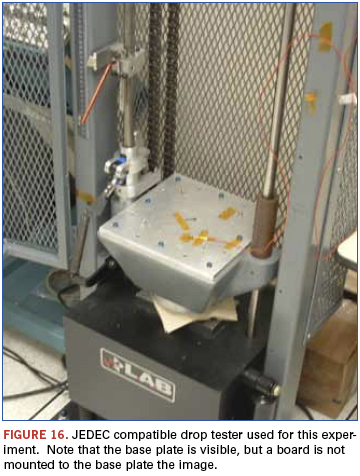
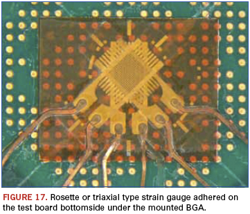
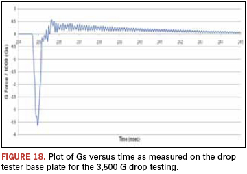
JEDEC drop testing. Drop testing was carried out using a JEDEC-compatible drop tester (Figure 16). During the drop, continuity to the daisy-chain parts was continually measured using a high-speed event detector. Additionally, triaxial strain gauges were affixed to the PCB on the bottomside of the BGA footprint to measure strain during the drop (Figure 17). Boards were attached to the base plate on the drop tester using four steel standoffs in the board corners. The JEDEC standard calls for boards to be dropped to Condition B, which is 1,500 Gs, as measured on the base plate with a 0.5ms duration and half-sine pulse.
Two of the underfilmed boards and two of the non-underfilmed boards populated with five parts each were initially dropped 100 times at 1,500 Gs. No electrical failures were recorded on any of the four boards. It was decided to drop the remaining four boards to the maximum 120cm height on the drop tester to achieve failures in a reasonable amount of drops to enable assessment of the performance of the underfilm material. Dropping from this maximum height resulted in approximately 3,500 Gs being recorded on the accelerometer on the base plate. See Figure 18 for a typical accelerometer output during a 3,500 G drop. The 3,500 G drop also resulted in a maximum of approximately 1,500µm strain being recorded on the strain gauge under the mounted BGA. One non-underfilmed board was dropped 118 times and the other 140 times, resulting in four of the five parts failing on each board. The first of these failures was recorded at 20 drops. The number of 3,500 G drops to failure for these two non-underfilmed boards is plotted on Weibull axes (Figure 19).
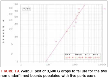
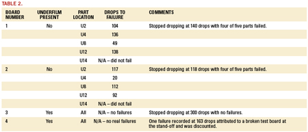
One underfilmed board was then dropped 300 times at 3,500 Gs with no failures recorded on any of the five parts. The intention was to drop the other underfilmed board 300 times, but following 163 drops, a failure was recorded on one of the underfilmed BGAs. The test board was inspected and was found to have broken in the corner where it attached to a standoff. The part that recorded the failure was located in the broken corner. This failure was discounted, and drop testing was terminated at this point. If a true failure had occurred on this board at this point, the underfilm material would have increased the drops to first failure by at least eight times (20 versus 160+ drops) versus non-underfilmed parts. If this second board had not experienced a PCB fracture and experienced no failures out to 300 drops as the other underfilmed board did, the underfilm material would have provided a 15 times improvement in drops to first failure. All 3,500 G drop test results are summarized in Table 2.
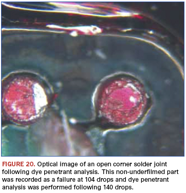
Drop testing failure analysis. A non-underfilmed part that had a failure at 104 drops was subjected to dye penetrant analysis following 140 drops.8 Typical solder joint fracturing was observed in the BGA corner (Figure 20). Since no true failures were recorded on any underfilmed parts, no analysis was performed on these.
Conclusions
A preform underfilm material designed to be a drop-in to the SMT process was evaluated for assembly characteristics, yield, drop test performance and thermal cycling reliability. The following conclusions were drawn from the study:
- The preform underfilm material was seen to be a drop-in to a conventional, high-volume SMT process and was handled and pick-and-placed very similar to discretes.
- Only a small design change was carried to the test PCB to accommodate the underfilm material. Tacky pads were added to the footprint to prevent any movement of the preforms prior to reflow.
- One hundred percent SMT assembly yield was achieved with 21,970 0.5mm pitch joints formed robustly on 65 BGAs containing the underfilm material. Following reflow, all BGAs with underfilm appeared to have the material adhered as expected between the BGA and the PCB in all four corners.
- The underfilm material had no observable effect on solder joint shape or standoff on the corner joints it came in contact with.
- Using a JEDEC-based drop test at a severe 3,500 Gs, drops to first failure was increased by a minimum of eight times and probably much greater (15 times or more) with the use of the underfilm material. An exact improvement factor could not be determined since no actual drop test failures were recorded with the underfilm material.
- Initial results suggest the underfilm material results in no degradation in thermal cycling performance. Thermal cycling to at least 50% failure continues.
Acknowledgments
The authors wish to acknowledge David Mendez and Kirk Kringel at Flextronics for technical and logistical assistance, Randy Temple and Dave Skupien at Alltemated for supplying the underfilm material along with applications assistance, Terry Burnette at Freescale for carrying out the rework evaluation, Scott Stoller at Freescale for performing the drop testing, Roy Arldt at Freescale for cross-sectional analysis and Ed Hall at Freescale for management support of this project.
References
1. JEDEC JEDS22-B111, “Board Level Drop Test Method of Components for Handheld Electronic Products”, July 2003, www.jedec.org.
2. C. Chiu, K. Zeng, R. Stierman, D. Edwards, and K.Ano, “Effect of Thermal Aging on Board Level Drop Reliability for Pb-free BGA Packages”, ECTC, p.1256, June, 2004.
3. D. Henderson, “On the question of SAC solder alloy – Cu pad solder joint fragility”, Webcast Meeting on SAC Solder Joint Fragility, Binghamton, NY, September, 2004.
4. S. K. Saha, S. Mathew and S. Canumalla, “Effect of Intermetallic Phases on Performance in a Mechanical Drop Environment: 96.5Sn3.5Ag Solder on Cu and Ni/Au Pad Finishes”, ECTC, S29p5, June, 2004.
5. M. Amagai, Y. Toyoda, T. Ohnishi, S. Akita, “High Drop Test Reliability: Lead-free Solders”, ECTC, S29p7, June 2004.
6. Alltemated Place-N-Bond Pick-and-Place Underfilm product data sheet, http://www.alltemated.com/img/Place-N-Bond-Underfilm-data-sheet.pdf?vsid=ypxrplzu.
7. W. Liu and N.-C. Lee, “Novel SACX Solders with Superior Drop Test Performance,” Proceedings of 2006 SMTA International, September 2006.
8. T. Burnette and T. Koschmieder, “Solder-Joint Failure Analysis”, Advanced Packaging, January 2003, pp. 25-27.
Ed: This article was first published at SMTA International in October 2011 and is reprinted here with permission of the authors.
The authors are with Freescale Semiconductor (freescale.com); This email address is being protected from spambots. You need JavaScript enabled to view it..