Despite competing goals of price and reliability, the technology requirements for most products are similar.
Ed.: This is the eighth of an occasional series by the authors of the 2019 iNEMI Roadmap. This information is excerpted from the roadmap, available from iNEMI (inemi.org/2019-roadmap-overview).
Medical electronics have historically been associated with high-cost diagnostic and imaging systems such as computed tomography scanners, magnetic resonance imaging, and ultrasound imaging, among other applications. Additionally, medical therapy devices like defibrillators, pacemakers and hearing aids have been marketed using value-based pricing. Neither of these medical electronics families were subject to aggressive cost reduction, and they all required high reliability.
Today, the focus in medical electronics is shifting out of the medical facilities to consumer access-based products, requiring technologies centered on portable diagnostics, remote patient monitoring and patient wellness therapy. This change in focus requires medical device manufacturers not only to meet aggressive reliability and performance requirements, but to also drive down cost for a broader, high-volume consumer market.
Two prominent differentiated medical electronics technology tiers are:
- Diagnostic and imaging systems: High cost, high reliability and low volume.
- Consumer-access portable diagnostics: Low cost, acceptable reliability and high volume.
Based on these two tiers, two opposing sets of goals bring products to market and manage the cost of ownership. The diagnostic and imaging systems business is well established. Companies like GE, Siemens and Philips have developed a methodology to design, qualify and manufacture these types of high-end systems, which are proven over many years for these types of products.
In the areas of consumer access portable diagnostics, cost challenges will dominate the approach to design, qualify and manufacture these types of products. Startup companies and major healthcare players must skillfully manage new platforms that empower customers to manage self-directed digital health and wellness.
The technology requirements for both tiers are similar. Many solutions are underway or in development, with a focus on the cost sensitivity for medical electronics’ mix of low, medium and high-volume products. Once these components and processes are developed and stabilized, they can be leveraged across medical electronics to meet industry needs and consumer demand. Several key enabling technologies are described briefly below.
Flexible carriers. Medical devices used for implantable, percutaneous, in-vivo or wearable applications often must accommodate size constraints and atypical form factors. Advanced flexible hybrid electronic (FHE) substrates, coupled with ultra-fine assembly, meet the challenge of miniaturization and unique form factor requirements. Ultra-thin flexible base polymer films, on the order of 12.5µm thick, have been fabricated for assemblies that can be rolled or folded into small volumes. Examples include highly miniaturized assemblies for use in a single-sided flexible module for an intravascular ultrasound catheter, and a double-sided flexible device used as an in-vivo diagnostic device.
Reduced lines and spaces. Semi-additive plating can produce fine-line circuit features that are key building blocks for miniaturization. This process (or pattern plating) provides the surface mount and interconnection pathways for passive and active electronic devices on a substrate. For double-sided flexible modules, electrical interconnection between the two sides of a base polymer flexible film is achieved using laser-drilled and copper-plated through-holes. Electroplating may be preceded by sputter deposition of a chromium tie layer (to promote adhesion between the metal and the polymer surface) and a copper seed layer. A smooth copper-polymer interface is ideal for this fine-line circuitry. Semi-additive plating provides a uniform cross-section that is scalable to line widths thinner than 10µm. Other advantages of the semi-additive process include higher metal trace aspect ratios than can typically be achieved using subtractive metal patterning.
Flexible circuit materials. Appropriate materials and surface preparation are vital to ensure good circuit metal adhesion. Polyimide films are traditionally a good choice as a base polymer material for these applications. The material offers excellent thermal durability at temperatures as high as 400°C. This mitigates issues of degradation in polymer properties, for example, induced by sintering of ink-jet printed circuit features or during solder reflow for component assembly.
One major caveat for medical device manufacturers is some polyimide manufacturers may be reluctant to permit their products to be used in certain medical applications. Those meant for permanent implantation in the human body or permanent contact with human body fluids or tissues are subject to supplier review. Risk management strategies may be in place to control which applications use the material. Medical applications that present only transient or minimal contact with human body fluids or tissues are more likely to meet supplier risk management conditions.
Liquid crystal polymer (LCP) is another high-performance, flexible circuit material with excellent thermomechanical properties. It can be thermoformed (even as a complex multilayer flex with embedded thin film traces) to any desired shape. Challenges regarding metal adhesion to LCP have been largely overcome. It is possible to manufacture high-performance flexible circuits using LCP.
High-density interposers. An interposer is an electrical interface often used to route a connection to a wider pitch. Two basic types of interposers (or substrates) are common. The first is a standard laminate multilayer substrate made using conventional PCB technology. The dielectric material may be a standard FR4 type using subtractive etching of the copper to form the circuitry. These substrates typically have plated through-holes that have been drilled using standard mechanical drilling methods. These substrates have as few as two layers or more to meet functionality needs in higher-performance devices.
Another type of interposer (often used for flip-chip attach) is the buildup substrate. In this design, a standard laminate core is used, most often two or four copper layers with PTHs. Buildup layers are added to both sides of the substrate to create up to 12 layers on each side. Buildup substrates enable the fine-line circuitry to fan out the high-density area array I/Os on the flip-chip die to a coarser pitch.
3-D chip stacking. Three-dimensional chip stacking can be accomplished using different techniques. A common technique utilizes stacked die with conventional wire bonding. Another approach uses silicon die having through silicon vias (TSVs) attached using solder cap copper pillars. This is commonly used to stack memory die on a laminate substrate. A newer stacked die methodology uses TSVs in the silicon substrate to be able to stack die directly on top of each other. This is accomplished using a TSV that is Cu-plated and allows communication directly through the Si substrate. The TSV eliminates the need for wire bonding, and the distance is much smaller than a wire bond, reducing the time for the signal to travel, therefore improving overall performance.
Fan-out wafer-level packaging (FOWLP). FOWLP produces very low-profile packages at a low cost. For instance, attaching a processor die directly to the redistribution layer (RDL) creates a very thin low-profile package. The entire first-level solder attach and underfill process steps are eliminated. Copper-filled TSVs connect the solder ball to the top memory module in a package-on-package configuration.
FOWLP may also be used to package multiple die. FIGURE 1 shows a system-in-package made by integrating different die types and interconnecting them with an RDL. In the mold example, die are placed on a carrier with a tape that has a thermal release layer. The die are then overmolded and the carrier removed. An RDL is applied on the surface of the die and solder balls attached. This is the most common approach used today. However, another RDL first approach is possible. The main difference here is the die are solder-attached to the carrier, which requires additional steps of solder attach and underfill.
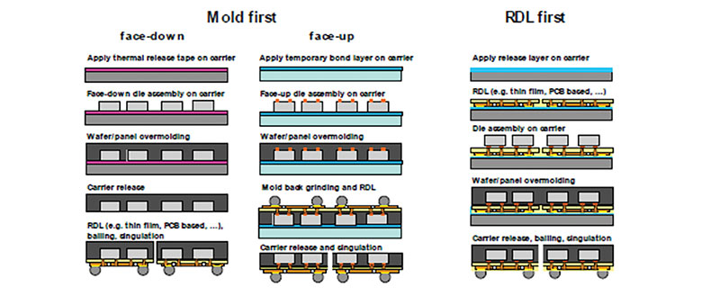
Figure 1. Multiple-die FOWLP package process flow options. (Source: Fraunhofer Institute1)
The industry is pushing developments in all these areas, with a view to cost-effective miniaturization of medical electronics and enabling increased functionality in future products across all segments.
References
1. T. Braun, et al, Fraunhofer Institute for Reliability and Microintegration, “Fan-Out Wafer and Panel Level Packaging as Packaging Platform for Heterogeneous Integration,” Micromachines (Basel), Special Issue Smart Miniaturised Energy Harvesting, published online May 23, 2019, ncbi.nlm.nih.gov/pmc/articles/PMC6562530/.
This article was excerpted from the Medical Product Emulator Group (PEG) chapter of the 2019 iNEMI Roadmap, chaired by Don Banks (Abbott, retired).


