ECAD-MCAD collaboration supports bidirectional communication that can shorten design times, reduce errors and bring competitive products to market faster.
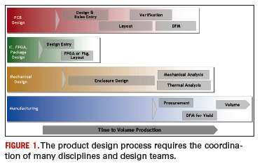
Product development requires a coordinated effort by many members of multiple disciplined design teams. We tend to focus on the design of the PCB, which is an extremely important element of the product, but it takes more than just the PCB to put a product into the marketplace (FIGURE 1). Many products require custom IC design or multiple FPGAs, software must be written and tested on the hardware and a mechanical enclosure, backplane and display must be designed; everything has to fit together with the PCB. Manufacturing the entire product must involve all members in the design process to ensure that the product can quickly reach production volumes and hit the target market window.

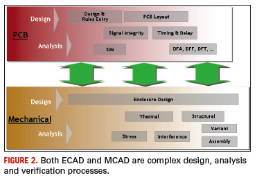
One of the most important aspects of designing a product is to coordinate the design of the PCB and the enclosure. Performing these designs in parallel, with constant communication between the disciplines, is absolutely necessary to achieve the most compact, highest-performance and highest-reliability end product while reaching the market window without extensive prototyping and re-spins. Both the electronics design (ECAD) and the mechanical enclosure design (MCAD) are very complex processes (FIGURE 2) requiring not just the physical design, but also many types of analysis and simulation, and the respective designs are highly related. For example, a change to the PCB can affect the mechanical enclosure or the cooling of the electronics in the enclosure, both mechanical design problems.

Collaboration Required
Collaboration is the bidirectional communication of information with the opportunity to negotiate a proposal. Collaboration between ECAD and MCAD has existed as long a product design has; it originated as paper being passed back and forth. Standards have been developed to take en masse data dumps from one domain into the other. For example, at the beginning of the PCB design process, IDF or DXF standard format data was used to transfer the board outline, mounting holes and keepouts (a result of the initial enclosure design) from the MCAD system into the PCB design system. After component placement, these same formats were used to transfer the component placements from ECAD to MCAD.
Years later, many ECAD vendors developed 3D viewers that allowed the enclosure to be viewed in the PCB design domain. Gross interference checking could then be preformed, but none of these capabilities provided for true, automated collaboration, i.e. the bi-directional communication of incremental change proposals with the facility to electronically negotiate between the domains.
New Standard Was Required
The first step was to develop, along with the ProSTEP iVIP Association, an ECAD–MCAD collaboration language standard. Rather than attempting to completely change the basic data models of both domains, a subset of objects was chosen and prioritized that represented those most likely to change during the concurrent design of the enclosure and PCBs. Examples included mounting holes, board outline, component parts and placements and height restrictions. Each of these object’s names, properties and constructs was specified to a mutually agreeable form so that both domains could fully understand them. Electrical Design-Mechanical Design (EDMD) schema represented the first true interchange format expressing incremental changes to a design that both domains could readily view, test and update in their respective databases. This standard was approved and published by the ProSTEP iVIP Association in May of 2008. The industry now had a common language covering the most important collaboration objects.
Real World Example
During product design and development, especially one with a high density of electronics in a small enclosure, the cooling of the electronics is a significant problem. Factors that can affect good or poor cooling are the placement of the components on the PCBs, the air flow through the enclosure, the conduction of the heat through escape routes, placement of heat sinks or fins on components, etc. So a typical design of a product may proceed as follows.
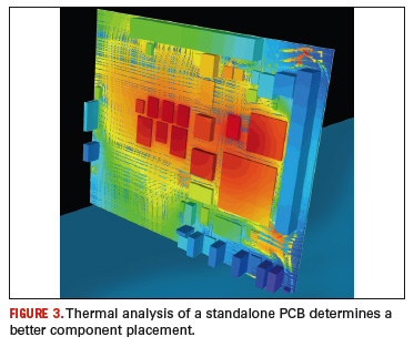
The mechanical designer designs the enclosure and through en masse data transfer, passes the board outline, hole locations, height restrictions, etc., to the PCB designer. The PCB designer performs an initial placement of the components on the board and passes that placement back to the mechanical designer again via IDF or DXF en masse data transfer. Testing and verification of the current design proceeds in parallel in both domains. While the mechanical designer analyzes the design of the PCBs in the enclosure, the designer might use a thermal analysis tool to analyze the PCB for cooling and junction temperatures. This analysis considers one PCB at a time and estimates the airflow or conduction from the PCB. Based on the analysis, the designer might decide to change the location of a hot component to improve the cooling.
That component location change is then incrementally communicated to the mechanical designer through the ECAD-MCAD collaboration software. The mechanical designer now has the opportunity to test that proposed change prior to accepting it. The placement change might cause interference with the enclosure, or the change might not be optimum for electronic cooling once included with the other PCBs in the enclosure.
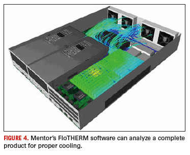
Using full enclosure thermal analysis, the MCAD designer is able to analyze the proposed change, including the fans, heat sinks, air flow obstacles and all the features of the full product (FIGURE 3). This type of analysis requires very sophisticated modeling of the elements. Since the PCB’s copper traces and power/ground planes offer excellent paths for heat conduction, accurate thermal analysis software can model multiple layers of the PCBs. Computational Fluid Dynamics algorithms are used to determine airflow from fans and even liquid cooling systems. The enclosure details and the mounting of the PCBs and other elements come directly from the mechanical design system and are included in the model.

The result (FIGURE 4) is a full analysis of the product, including the proposed component location change to the PCB. The mechanical engineer can then review the change and if it is acceptable, using the ECAD-MCAD collaborator, the mechanical engineer can communicate this acceptance back to the PCB designer. The change is then reflected in the respective databases.

Where Do We Go From Here?
We have discussed just one example of how collaboration is required between the various disciplines involved in the design of an electronics product. Users and their ECAD and MCAD design software suppliers drove this particular example. It established a new standard, open and available to the industry. The ECAD-MCAD collaboration capability can now electronically support the bidirectional communication and negotiation of incremental changes, thus providing the opportunity for reducing design times, reducing errors and bringing more competitive products to market.
But other opportunities exist and must be addressed as we consider that the design of the product is more than the PCB and the mechanical enclosure. From the designer’s perspective, additional collaboration between the domain and the other disciplines (manufacturing, procurement, ASIC/Package, FPGA, software, etc.) in the product design process can only mean better profits for their companies. PCD&F
John Isaac is the director of systems market development, Systems Design Division at Mentor Graphics Corporation and can be reached at This email address is being protected from spambots. You need JavaScript enabled to view it..


