Vikram Jandhyala, Dipanjan Gope, Swagato Chakraborty, Feng Ling, Xiren Wang, Devan Williams and James Pingenot
Advanced computing languages will help to develop flexible solver architectures and efficient simulation methods.
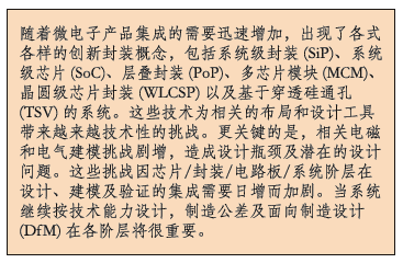
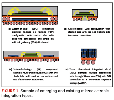
The rapidly growing needs of microelectronics integration have resulted in a mind-boggling variety of innovative packaging concepts. Some of these package types can be seen in FIGURE 1. These technologies create an increasing technical challenge for related layout and design tools, and more critically, the associated electromagnetic and electrical modeling challenges are rising exponentially and creating design bottlenecks and potential design gaps. These challenges are exacerbated by the growing need for integration across chip-package-board-system hierarchies in terms of design, modeling and verification.

The concept of an SoC includes multiple chip functionality, as well as digital, analog and mixed-signal functions in a single chip-level system with all associated integration and packaging. In FIGURE 1a, an SoC component comprised of two bond-wire connected dies on one package and a BGA-connected die on another package, stacked in a PoP configuration are shown. Such geometries and connectivities lead to complex electromagnetic situations required to obtain broadband electrical models. In FIGURE 1b, a different approach to stacked die, often used in memory applications, is depicted. In this case, the bond-wires are situated on the top and bottom layers, and a cut is created through the package/printed circuit board to route the bond wires. This can create electromagnetic issues. In FIGURE 1c, multiple dies and stacked dies are connected to a single package layer, potentially creating chip-to-chip crosstalk if not accounted for appropriately. Finally, in FIGURE 1d, 3 DICs are stacked together and routed using TSVs, a recently-developed innovation for WLCSPs and 3 DICs applications.
While Figure 1 depicts system-level integration, electromagnetic issues are found at every level of hierarchy. For example, the inclusion of chip effects, necessitated by recent requirements by designers of integrated chip-package-board co-design, drastically changes the requirements on electromagnetic solvers. Several scenarios arise for on-chip electromagnetic modeling. These vary from standard resistance-capacitance extraction for on-chip nets to the inclusion of inductance to modeling of full-wave electromagnetic effects for analog on-chip integrated passives. The presence of digital and analog components and sub-systems necessitates modeling the effect of mixed-signal coupling from high-speed digital sections to sensitive analog subsystems. In addition, the connection of chip-to-package via bond wires, or BGA, creates its own coupling challenge. Redistribution layers (RDL) are required to appropriately connect on-chip signal and power nets to bond wires. Similarly, the locations of on-chip I/O pads for BGA connections need to be optimized to minimize certain metrics such as inductive coupling in power nets. Integrating these geometric intricacies and multi-scale features with all the associated electromagnetic effects from package and board-level interactions is an added challenge for co-design.
Electromagnetic Modeling Challenges
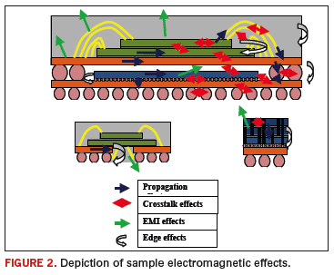
FIGURE 2 depicts instances of the varied electromagnetic (EM) effects that are encountered in chip-package-board co-design. Whether the ultimate goal is power integrity (PI), signal integrity (SI) or electromagnetic interference (EMI) prediction, these EM effects have critical roles to play. The first order effects for signal (and power) propagation are shown by blue arrows. Within the confines of a digital chip, propagation along horizontal (traces) and vertical (via) structures needs to be modeled, including possible reflection at discontinuities and transitions. In an analog, radio frequency (RF) or mixed signal chip, the propagation modeling needs additional detail to model high-frequency effects such as through an on-chip inductor or filter. Once the signal leaves the chip, the propagation (and reflection) is effected by discontinuities at the RDL layer or I/O pad where the signal enters a BGA or bond wire. The signal then encounters another discontinuity on the other side of the connection, at the package (or PCB in a CoB) side. Once the signal enters the package, the dominant propagation through traces and vias is affected by reflections caused by impedance discontinuities including layer changes, antipads and voids and path dimension changes. Finally, impedance discontinuities may be encountered at the solder balls.

Multi-port impedance, admittance or scattering-matrix models that can be used by circuit simulators are directly affected by the dominant first order path effects. In particular, self-terms that account for reflection and transmission along a specific net (connected metal) are highly dependent on these first order effects. The remainder of the models is populated by crosstalk terms that are typically undesirable but are produced by electromagnetic coupling.
In Figure 2, the red arrows depict EM crosstalk mechanisms. Within the chip, cross coupling between traces is an example of crosstalk. There may also be crosstalk between different metal layers on the same chip or even between two stacked dies, depending on the orientation and the silicon thicknesses. When the signal emerges from the chip, there is possible crosstalk at the I/O pads, RDL layer and between C4 bumps. Crosstalk between bond wires presents itself both for signals from the same chip and from different chips, as in a stacked die case. There are significant crosstalk mechanisms in the package and PCB that must be accounted for. Trace-trace coupling, via-trace coupling, via-via coupling, coupling paths through voids and antipads, current return path spreading (for example with plane discontinuous as shown in the CoB case) and discontinuities are all contributive.
Loss is a critical factor for both propagation and crosstalk. All metal that has excited or induced current impressed upon it will be susceptible to ohmic loss. The loss will also increase with frequency (skin effect) and with the vicinity of other metal (proximity effect). Every dielectric material also has an associated loss, related to the imaginary part of its electrical permittivity, which will increase with frequency to the point where it may even become dominant in the GHz range.
As the number, type and functionality of wireless components, systems and protocols has increased, the need for minimizing through-the-air EM interference has also increased–whether through the demands of regulatory bodies such as the FCC (EMC or electromagnetic compatibility) or by actual interference-causing, self-interference or cross-interference with other systems (EMI or electromagnetic interference). Along with SI and PI, the need to also account for EMI is achieving critical levels. EMI mechanisms of radiation are represented by green arrows. Top-layers of chip, bond wires, package layers and traces are all potentially strong sources of EMI. This is particularly true if systems are either not designed to have differential excitation and ports (which tend to have low radiation due to cancellation of fields) or have excessive asymmetry resulting in common mode generation even under differential design (tends to happen due to a variety of geometrical effects including boundaries, voids, path lengths, impedance profiles and mismatches, non-parallel paths, etc.).
Edge effects are created by abrupt boundaries and may give rise to impedance mismatches (critical in power integrity), reflections (critical in signal integrity) and radiation (critical in EMI). It is important that these effects also be modeled accurately. The gray-white arrows show some examples; external boundaries of chips, packages and PCBs cause edge effects. Boundaries of metal planes within these structures also give rise to the same effect. Abrupt edges of material layers, such as the epoxy layer shown, can also cause edge effects. Importantly, internal discontinuities within planes, such as large slots or separate power planes, also yield strong edge effects. These effects can range from fringe capacitance through impedance mismatches to radiation, and they need to be accounted for in generating models for SI, PI or EMI.
We may be approaching a limit on the clock frequencies of individual digital cores. With the advent of multi-core systems and the mushrooming of mixed-signal, analog and RF systems at multi-gigahertz frequencies, the throughput of signals through these systems is continually on the rise. The ever-increasing speed and frequencies of chip-package-board-systems, unfortunately, has a deleterious effect on the electromagnetic scenario. Practically every EM phenomenon gets more involved as frequencies and speeds increase. Skin effect forces current to travel through smaller cross-sections and rapidly increases the loss and resistance with frequency. Dimensions of geometries become electrically larger as frequencies increase, and more sections of the system become efficient radiators, thereby increasing EMI, crosstalk and radiation loss.
Simple approximations, such as transmission line models, transverse EM (TEM) models and lumped models, also become drastically inaccurate. Dielectric materials start behaving in an increasingly lossy and frequency-dependent manner, causing signal distortion and loss through dispersion and attenuation. Even for power integrity applications, with power signals near DC, switching effects on multi-GHz frequency rise times are now common and necessitate high-frequency modeling even for PI problems. It is clear that SI-PI-EMI is moving into the arena where full-wave, 3D electromagnetic modeling is a necessity and simpler, more efficient approximations are becoming irrelevant. Designers need to be aware that such approximations may produce results that have no basis in reality for design or verification.
Electromagnetic Modeling Approaches
3D Resistance Extraction. This entails the solution of either a resistive network problem involving digital chip layers or modeling substrate losses. While this requires modeling of full 3D geometry, it is a relatively simple computation.
3D RC Extraction. The next level of complexity involves creating 3D RC models for chip metal layers and substrates, obtained by solving Poisson’s equation. The models are suitable for timing and delay computations and for on-chip signal integrity and power distribution networks at relatively low clock frequencies.
3D RLC Extraction. On-chip modeling at GHz frequencies necessitates the modeling of inductance in addition to RC modeling. The potentially distributed nature of inductance loops, as well as frequency dependence due to skin and proximity effects, makes this a significantly more involved problem, but very relevant for on-chip modeling.
3D Quasi-Static Modeling. This technique of modeling has at one end RLC modeling at the package level. In a more complex version, the R, L and C are coupled and derived from the same solution. The phase term (occurring in Green’s functions) is ignored during full-wave modeling. Physically, this is equivalent to assuming all influences (currents, voltages, fields) travel instantaneously through the system. Quasi-static models are widespread for full-port electrical models for packages. These typically have validity up to the low GHz range and are used for both power integrity and signal integrity.
2D Transmission Line Modeling. This is traditionally a very useful technique when there are significant symmetries and structures present in the problem. For example, well-designed parallel PCB traces over a ground plane can be modeled very well with per-unit-length (2D cross section) RLGC parameters. These have restricted validity for more general propagation paths and need book-keeping and corrections when traces pass over voids, bend, connect to vias, change their width, have impedance discontinuities, etc. This technique primarily focuses on differentially excited, symmetric structures.
2.5D TEM Approximations. When electromagnetic fields are localized to flow between parallel metallic plates with small gaps relative to wavelength, transverse electromagnetic approximations are valid. Such an approach is termed to be of 2.5 dimensions and has been used successfully, primarily for power integrity modeling.
2.5D Layered Approximations. For on-chip RF, analog and mixed-signal components such as embedded passives (filters, inductors, transformers, etc), the relative sizes of the components are small when compared to the lateral extent of the dielectric layers. In this case, layered infinite (in transverse directions) approximations make the solution efficient and accurate, and 2.5D-layered method-of-moments techniques can be used. This also has applicability on some subsets of PCB modeling, but it is generally inapplicable there and on packages where 3D edge effects are important.
3D Full-Wave Modeling. This represents the most accurate approach to EM modeling of chip-package-board-systems. There are significant challenges to achieving this goal in terms of scale, memory and time while preserving the expected accuracy of 3D full-wave modeling. There are three main techniques that are considered to be the workhorses of this area, and most successful commercial solvers are built around highly efficient versions of these techniques. The finite element method (FEM), initially used in civil engineering, is a staple of 3D full-wave modeling. It is a general technique that uses volumetric meshes to convert the partial differential equation (PDE) form of Maxwell’s equations in the frequency domain to a large, sparse matrix equation.
Challenges of Inputs to EM Solvers. Chip-package-board-system models need to be prepared for analysis by EM solvers. This typically means integrating several different file formats. Net identification, port definition and boundary condition specification (especially in FEM and FDTD where this is not automatic) are also needed prior to solution.
Challenges of Outputs from EM Solvers. Even with complex EM solvers that may solve part of or the entire simulation problem, the appropriate outputs are critical. In particular, S-parameter, impedance or admittance matrices are useful to understand propagation and coupling in systems. However, for circuit-level simulation, circuit models need to be generated from these matrices. These models need to be passive and causal in order to ensure that the circuit outputs are accurate and stable. Impedance profiles and time-domain reflection/transmission plots are also required.
Recent Advances
Advances in computing platforms, coupled with recent breakthrough in algorithms, have dramatically changed the picture in 3D EM simulation for chip-package-board-system co-design. In particular, MoM techniques, that typically were restricted to 2.5D-layered solvers, have recently become extremely powerful due to advanced multi-scale algorithms. These techniques accelerate the iterative solution of MoM matrices by replacing the quadratic cost of matrix-vector products with near-linear costs in the size of the system matrix–which in turn is dependent on the number of mesh elements. This linear scaling, in terms of solution time and memory, is particularly attractive for large structures such as integrated chip-package-board-systems. In addition, these multi-scale algorithms are also amenable to parallelization on shared memory systems; the entire matrix-vector product is parallelized over multicore CPUs. These three techniques will continue to be the mainstay of 3D EM simulation for chip-package-board-systems.
Emerging Needs and Future Directions
With rapid advances in solver technology, focus is now shifting towards true design tools. These tools will enable fast parametric simulation in a large number of parameters enabling what-if analysis and early design. Tunable accuracy and precision will also enable early design optimization. As systems continue to be designed at the edge of technological capabilities, manufacturing tolerances and design for manufacturing (DfM) will be critical at all levels of hierarchy. Statistical modeling, mean-variance and higher-order variability measures, probability distributions and yield estimates will all be critical– both in a standalone manner and in the context of robust optimization. Optimization will rely on multiple objectives and multiple parameters, requiring extremely efficient solvers as well as visualization and graphing techniques. Eventually, advances in computing languages will allow the development of more flexible-solver architectures that will determine the most efficient simulation method for a specified accuracy or a subset of the entire problem. These needs and directions are sure to keep designers, design automation tool developers and researchers in excited and busy for years to come. PCD&F
Dr. Vikram Jandhyala is CEO and founder of Physware, Inc. He is also an associate professor in the department of electrical engineering, University of Washington, Seattle and director of the applied computational engineering lab there. He can be reached at This email address is being protected from spambots. You need JavaScript enabled to view it.. Dr. Dipanjan Gope is VP of research and development, Dr. Feng Ling is VP of engineering, Dr. Xiren Wang is a research and development engineer, Dr. Swagato Chakraborty is the VP of products, Devan Williams is a senior research and development engineer and James Pingenot is a senior research and development engineer, all working for Physware, Inc.


