Advanced materials provide a low cost and highly versatile method for manufacturing flexible electronic circuits.
Printing technologies provide a simple solution to build electronic circuits on low-cost flexible substrates. Nanocomposites will play an important role for developing advanced printable technology.
A variety of printable nanomaterials for electronic packaging have been developed. This includes nanocapacitors and resistors as embedded passives, nanomagnetic materials, multifunctional materials, etc. Nanocomposites can provide high capacitance densities, ranging from 5nf/inch2 to 25 nF/inch2, depending on composition, particle size and film thickness. The electrical properties of capacitors fabricated from BaTiO3-epoxy nanocomposites showed a stable capacitance and low loss over a temperature range from 25ºC to 100ºC.
In recent years, significant progress has been achieved in the development of semiconductor packaging technology using various printing methods such as screen-printing, ink-jet printing and microcontact printing. This trend is driven by demand for low-cost, large area, flexible and lightweight devices.
Since printing is inherently additive in nature, material and disposal costs are expected to be reduced, resulting in an extremely low-net system cost. Most of the research activities in this printable area have been devoted to developing ink-jet, solution-processable conductor materials.1-4 Printable materials need to be chemically and physically inert to the other functional, dielectric and photoimageable materials processing in the same layer to preserve the structural and electrical integrity of devices/packages, and they have to be operationally stable to sustain long operation life. For these purposes, organic and polymeric materials have been widely pursued since they offer numerous advantages, including low-temperature processing, compatibility with organic substrates, stability and significant opportunity for structural modification.
Nanocomposites provide the greatest potential benefit for high-density, high-speed, miniaturized advanced packaging. The small dimensions, strength and the remarkable physical and electrical properties of these structures make them very unique materials with a range of promising applications.
Semiconductor devices based on nanocomposites are considered to be very promising for electronic applications since they may potentially be fabricated entirely using similar printable polymer technologies where different active fillers can be introduced within the same functional polymer system. Several nanocomposites have been reported for advanced packaging applications. There is room for improvement of the existing materials, so that low processing temperatures, flexible and cost-effective printable processes and materials can be developed for large-scale production.
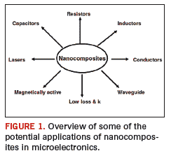
Novel printable nanocomposites have the potential to surpass conventional composites to produce materials, structures, manufacturing and circuit applications compatible with laminated organic substrates. An electronic application of a printable nanocomposite such as conductive adhesives, interlayer dielectrics (low-k, low loss dielectrics), embedded passives (capacitors, resistors) and circuits can be seen in Figure 1. In addition, printable optically/magnetically active nanocomposites and polymeric materials are being investigated for use in the fabrication of devices such as inductors, embedded lasers and optical interconnects. Here we have used epoxies as the typical polymer matrix and a range of metal/ceramic fillers with particle size ranging from 10 nm to 10 microns. The addition of different fillers into the epoxy matrix controls the overall electrical properties of the composites. For example, the addition of zinc oxide nanoparticles into the epoxy shows laser-like behavior upon optical pumping. The addition of barium titanate (BaTiO3) nanoparticles results in high capacitance. Thermosetting resins in general have advantages in terms of manufacturability, processing temperatures, low moisture absorption, high glass transition temperatures (Tg) and versatility, making them quite promising for advanced packaging. However, homogeneous dispersions of ceramic particles in the epoxy matrix are a critical step to achieve uniform property films.

Printable nanocomposites have potential applications at all levels of microelectronics (see Figure 1). Printing processes have several advantages such as selective deposition, repair and re-print capability. However, printed features with desired properties, thickness and tolerance present significant challenges. In general, nanocomposite solutions are used for thin ink-jet printing, and pastes are used for thick screen and contact printing.
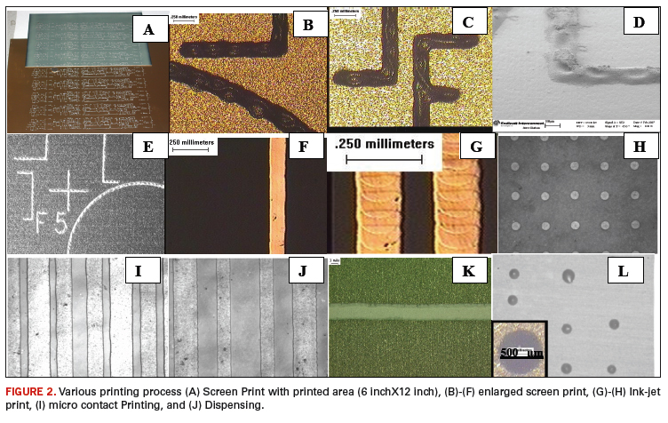
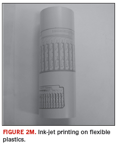
Nanocomposite concentration and corresponding viscosity is important for the printing process. Ink-jet printing prefers low viscosity in the range of 7 cp to 10 cp. Low viscosity helps to generate submicron thin structure. Screen and contact printing prefer higher viscosity (100,000 cp to 150,000 cp) thixotropes and generate 10 to 25 micron thick features. Conducting polymers/composites favor ink-jet printing for transistors but can use screen/contact printing for making lasers, which is a surface phenomenon where surface particles upon optical pumping show laser-like behavior. Embedded resistors, capacitors and conducting circuit lines can use ink-jet or screen-printing for different features. Dielectric features are typically large and can use any of the known print techniques. Figure 2 shows various printings. Figures 2A-E represent the screen-printing process. It can be seen that screen print methods can produce line features in the range of 100 microns. Figures 2F-J represent ink-jet printings showing minimum line feature size in the range of 75 to 100 microns and ~50 microns dot patterned. Space between two ink-jet printed lines can be reduced to 50 microns. Figure 2K represents micro-contact printing with minimum feature size around 100 microns. For the dispensing technique, feature sizes depend upon the material viscosity and corresponding needle used to dispense materials. It can dispense different shapes with a minimum dot of around 20 mils (500 microns) (Figure 2L). In addition, we are developing flexible packages for a variety of applications. Several classes of flexible materials can be used to form high-performance flexible packaging. We are investigating ink-jet printing for low-cost flexible packages. Figure 2M represents ink-jet printing on flexible substrates.

Capacitors and Resistors
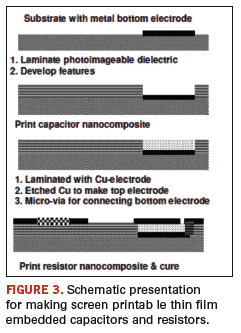
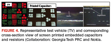
Novel classes of polymer nanocomposites that have shown a high dielectric constant are the BaTiO3 epoxy nanocomposites. These are used to fabricate thin-film embedded capacitors. High temperature/pressure lamination was used to embed capacitors in multilayer PCBs. The capacitor fabrication is based on a sequential build-up technology employing a first-etched copper electrode. After patterning of the electrode, the nanocomposite can be deposited and laminated within a PCB. Nanocomposites can be directly deposited by printing. Figure 3 shows a process flow for making screen-printed, discrete embedded capacitors and resistors. Capacitance values are defined by the feature size, thickness and dielectric constant of the polymer-ceramic compositions. Figure 4 shows a representative test vehicle (TV) and corresponding cross-sectional views of screen printed embedded capacitors and resistors. Measurement of electrical properties of capacitors fabricated from nanocomposite prints and with areas of ~2 mm2 to 100 mm2 (smallest circle electrode 0.060” diameter and square was 0.109” x 0.109”) showed high capacitance density ranging from 5 nF/in.2 to 25 nF/in.2, depending on composition, particle size and thickness of the prints. Thin-film capacitors fabricated from 40% to 60% v/v BaTiO3 epoxy nanocomposites showed a stable capacitance density in the range of 5 nF/in to 20 nF/in.2 and low loss ~0.012 to 0.022. Measurement of electrical properties of capacitors fabricated from 70% v/v nanocomposite showed capacitance density of about 25 nF/in.2. Capacitance density of BaTiO3-epoxy polymer nanocomposites modified with nanomaterial was also investigated. Capacitance density of nanomaterials with modified films was higher than BaTiO3-epoxy nanocomposites.


Nanococomposites are attractive for resistor applications because variable resistor materials can be formed simply by changing the metal insulator ratio. These compositions, however, have practical advantage only when they are capable of being printed in the internal layers of circuit boards. We have developed various discrete resistors with a sheet resistance ranging from 1 ohm to 120 M ohm. Resistors in various ranges (e.g. 1, 5, 10, 50 and 100 ohms) can easily be made. Resistor materials can be printed in the same internal layer. Figure 5 shows printed resistors with different lines and spaces.

Inductors
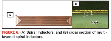
Ink-jet printing of spiral structures can be used to form inductors. The spacing in the spiral and resistance will dictate quality of inductors. High resistance causes thermal loss and, therefore, is not suitable for inductors. In this example, we deposited multi-metal layers on ink-jet printed lines to increase current carrying capacity or conductance. High conductance spirals can generate a higher magnetic field at the same voltage, thus providing a higher inductance in smaller packages. We used a variety of multi-metal layers including electroless copper, immersion gold, electroless gold, electroless palladium, electroless nickel and others. Figure 6 shows a representative example of multi-metal-layer-based inductors. Multi-metal layer deposition reduces line resistance to hundreds of milliohms.

Reliability
Reliability of the nanocomposites was ascertained using IR reflow, thermal cycling, the pressure cooker test (PCT) and solder shock. The change in capacitance after three times in IR reflow and after 1,000 cycles of deep thermal cycling (DTC) between -55ºC and 125ºC was within 5%. The change in capacitance after IR reflow (assembly) pre-conditioning (3X, 245ºC) and a thermal shock up to 1,400 cycles (-55C to 125ºC) for large, medium and small embedded capacitors was less than 5% (Figure 7). Most of the nanocomposites in the test vehicle were stable after IR reflow, PCT and solder shock. The change of conductivity of electrically conducting adhesives after 3X IR reflow at 220ºC was less than 5%. Some of the low-loss materials were also exposed to PCT (4 hr.) followed by a 15 second solder dip at 260ºC. PCT and solder shock sometimes cause delamination. In general, solder dip/shock pick up the PCT-induced defects and cause delamination. Initial PCT - solder dip experiment didn’t show any delamination. Detailed reliability testing of nanocomposites is under investigation.

Conclusion
Printable nanocomposites are promising – because they are not only versatile – but also economical when compared to other methods. A variety of nanocomposites suitable in printable processes for the fabrication of selective and localized embedded components in PCB/LCC has been developed. The materials and processes enable fine features and controlled thickness layer deposition. This is accomplished by using ink-jetting, screen printing, contact and dispensing processes.
Nanocomposites can produce variable resistances ranging from 1 ohm to 120 M ohms. Low k and loss materials can also be fabricated from nanocomposites. Overall, printable nanocomposites will be useful to produce multi-functional complex electronic packaging. The results also suggest that printable nanocomposites may be attractive for roll-to-roll manufacturing of large-area microelectronics, such as roll-up displays, E-papers, keyboards, radio frequency structures and medical devices. PCD&F
References
1. G.B. Blanchet, C. R. Fincher, and F. Gao, “Polyaniline nanotube composites: A high-resolution printable conductor” Appl. Phys. Lett., Vol. 82, No. 8, 1291
2. D. Huang, F. Liao, S. Molesa, D. Redinger, and V. Subramanian, “Plastic-Compatible Low Resistance Printable Gold Nanoparticle Conductors for Flexible Electronics” Journal of The Electrochemical Society, 150 (7) G412-G417 (2003)
3. H-H Lee, K-S Chou, K-C Huang, “Inkjet printing of nanosized silver colloids” Nanotechnology 16 (2005) 2436–2441
4. Yiliang Wu, Yuning Li, Ping Liu, Sandra Gardner, and Beng S. Ong, “Studies of Gold Nanoparticles as Precursors to Printed Conductive Features for Thin-Film Transistors” Chem. Mater. 2006, 18, 4627-4632
Rabindra Das is senior advisory technologist, This email address is being protected from spambots. You need JavaScript enabled to view it., How Lin is senior advisory test engineer, This email address is being protected from spambots. You need JavaScript enabled to view it., John Lauffer is senior advisory technologist, This email address is being protected from spambots. You need JavaScript enabled to view it., Michael Rowlands is senior associate R&D engineer, This email address is being protected from spambots. You need JavaScript enabled to view it., Norman Card is associate process engineer, This email address is being protected from spambots. You need JavaScript enabled to view it. and Voya Markovich is senior VP & CTO, This email address is being protected from spambots. You need JavaScript enabled to view it., all working for Endicott Interconnect.
Ed note: This article is based on materials presented at the 2008 IPC Printed Circuit Expo and is printed with the permission of the authors.


