Note: Part 1 appeared in the September issue. Part 2 appeared in the October issue. Both parts are presented here.
PART 1
Microvias reduce layer count when routing high pin count BGAs.
Although I am unaware of any BGA with a pinpitch of 0.8 mm and over 1500 pins, the day will come when they replace the large 1mm devices. The FPGA companies who are approaching 2000 pins with 1-mm pin-pitch are correctly concerned about the transition to 0.8 mm. Exceeding 2000 pins with 1-mm pin-pitch results in a very large BGA that is not only more expensive to manufacture, but also more difficult to attach to the board due to potential warping of either the device or the board. The FPGA customers want increased functionality (resulting in more pins), yet they have no experience routing such a large and dense device.
Using the principles described previously for 1-mm BGAs, this three-article series will explore fanout and breakout solutions for routing the large 0.8-mm devices. This first article explores the use of through vias with FR-4.
For the purpose of testing, a footprint for a Virtex-5 with 1760 pins at 1mm pitch was converted to 0.8-mm pitch. There are 1227 I/Os that need to be escaped. The rest of the pins are power and ground.
Testing continued by applying fanout patterns using the North East South West (NSEW) method and applied breakout patterns for three different via configurations.
Test 1: Through Vias. The first test used only through-vias with the intent to demonstrate the number of layers required for such a method so it could be compared to the other more efficient solutions.
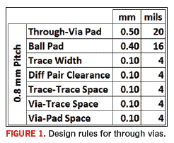
The design rules, as shown in Figure 1, for the first test are the same as used in the 1-mm pitch tests from the previous articles, except the ball pads are a little smaller due to the smaller pin-diameter and pin-pitch.

Test 1: Fanout Patterns. A common question question from designers is, "How can I reduce the layer count?”
If you are fortunate enough to work with the ASIC or FPGA designers, you can potentially have them organize all the perimeter pins so they are used for I/Os. This can reduce the layer count simply because more of the I/Os can be routed on the first signal layer.
Another method that applies to all BGAs that use through vias is to push the fanouts out and away from the perimeter of the ball pads. This technique allows for an extra two rows of I/Os to be routed on the first signal layer. In most cases, this will result in a reduction of one signal layer for escaping the BGA. One signal layer may not sound like much, but depending on your situation it may actually mean you can reduce the stackup by two signal layers just because the symmetry of the stackup require two layers to be added together.
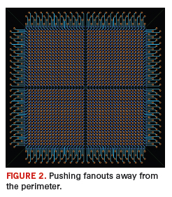
Figure 2 illustrates pushing the fanouts out and away from the perimeter. The intent was to move the vias far enough out so that three traces could be routed between them on the diagonal. In the center of the BGA, use a simple matrix dog-bone pattern that opens up the route channels in the center rows and columns.

Test 1: Breakout Results. When using the through via only, it took seven routing layers to accomplish the NSEW breakout. If the perimeter vias where not pushed out, it would have taken eight layers. If you work on every escape trace, packing them in with the maximum pain (PCB designers will know what I am talking about), then you may even be able to reduce the total layer count for escaping this 1760 pin (1227 I/ Os) device to six layers.
Unfortunately there isn’t much you can do to reduce layer count when using through via fanouts on these 0.8-mm BGAs. However, you can eliminate one to two layers with the above techniques. Using microvias will allow this BGA to be escaped in only five or even reduced further to three signal layers depending on the stackup and via methodology. These other methods will be explored in the next two articles of this series.
PART 2
Microvias can reduce the number of signal layers required.
This article focuses on increasing routing density using microvias. I took a footprint for a Virtex-5 with 1760 pins (1227 I/Os) at 1-mm pitch and converted it to 0.8-mm pitch as the basis for the tests.
Test 2: Stack-up. An HDI stack-up was used with 1:2 microvias, 1:3 skip-vias and a through via. The through via was used for fanout of the power and ground pins so they could attach to all the planes and the discrete components on the opposite side of the board. I chose the through via over a buried via because it turns out that the through via is the same size as the buried via would have to be, and the through via is more direct and simple.
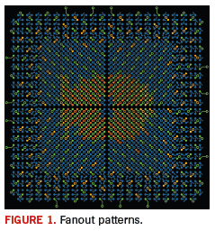
Test 2: Fanout Patterns. It appears that Figure 1 presents a different set of fanout patterns than previously described. However, a closer look shows that the same principles of aligning vias and combining different patterns are applied.

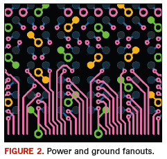
Test 2: Power and Ground. The power (orange) and ground (green) vias are all through vias. Around the perimeter, the ground fanouts have been added a distance away from the ball pads as shown in Figure 2. By doing this, an extra route channel is opened between the through vias and the microvias on layer two.

Test 2: I/O Pins. By using microvias around the perimeter, the effective size of the BGA (to be routed using through vias) has been reduced from 1760 pins to 784 pins.
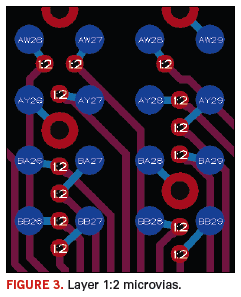
Test 2: Layer 1:2 Microvias. The 1:2 microvias are aligned in columns and rows between pairs of ball pads. Because of the 0.8-mm spacing between the ball pads and the rather large space that the through via takes, the microvias are not evenly spaced.
In Figure 3, the microvias at the top are not aligned in a column. This is because the through vias for the power and ground take up enough space that there isn’t room for the microvias to be aligned. This doesn’t affect the route density. Since there are no additional traces on layer two (purple traces) that have to come through that area, placing the vias horizontally doesn’t block any other traces. This is a general principle when placing the fanout vias.

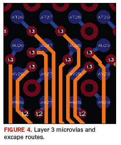
The layer 1:2 microvias are used for the first four rows of pins, and the layer 1:3 microvias are used for the next three rows of pins. Due to the through vias used for the eighth row of pins, the 1:3 microvias had to be packed into a smaller area. This means the 1:3 microvias are not aligned in columns, however, there is a pattern to the madness shown by the pattern in Figure 4.

Test 2: Breakout Results. Applying NSEW breakouts with good fanout patterns enables breakouts on large BGAs in five to six signal layers. This method can maintain normal trace widths and clearances. PCD&F
Charles Pfeil is an engineering director for Mentor Graphics, Systems Design Division. Email: This email address is being protected from spambots. You need JavaScript enabled to view it..


