Leveraging globalization allows electronics companies to meet business goals of improved time-to-market and lower development costs.
Globalization seems to be the buzzword of the electronics industry. The question is: what effects does this have on the electronic product development process? Can electronics companies still afford to use simple PCB systems design solutions, or are there better design solutions that must be adopted to maintain competitive parity? What new technologies and processes do designers have to learn? And how does the infrastructure of a company adapt to this changing world? These are critical questions in the face of globalization.
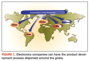
When we think of globalization, most of us immediately focus on the continuing move of manufacturing away from the US, Japan and Europe and into the Asia-Pacific and other low-cost manufacturing countries. But globalization is more than manufacturing. Many large electronics companies are not only using manufacturing in the Pac-Rim but are also establishing significant facilities in these countries to capitalize on the low-cost engineering talent that is available. They are also outsourcing design of all or parts of their products to ODMs (original design manufacturers). We now have a situation where the development and delivery process for a product may be spread across a number of locations around the world (FIGURE 1).

Another aspect of globalization is the necessity to market a product on a global basis. Companies need to design a product globally and then sell it to a global audience. This all adds new meaning (and words) to an old adage: “Design Everywhere – Build Anywhere – Sell Globally.” For a change, let’s work backward through the process.
Sell Globally
When a company produces a product for sale in various regions around the world, it often has to produce different versions of the same design. Examples might include different operating voltages for a product, different electromagnetic emissions regulations or different communication protocols for a wireless device depending on location. The less efficient and most risky way to meet these goals is to: design a specific product for each region, estimate the number of units to be sold in each region, and then manufacture and stockpile the correct number of units to be sold. The risk is you can produce more than enough for one region and not enough for another, thus wasting stock and missing market opportunity respectively. Another option is to slow down manufacturing and only produce versions as needed in the marketplace; again risking maximum sales due to the time required to re-kindle a manufacturing line to high volume.
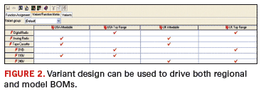
The best option is to use the method of “variant design.” Using this method, a single design is produced that will accommodate all of the possible variations required for the different regions. The variations are dependent on the combination of component(s) mounted and independent of the bare board. The bare boards can then be manufactured in high volumes and stockpiled. (The bare board is not nearly as expensive as the components that go on it.) Then depending on the specific volumes required for each region, have manufacturing assemble the boards with the correct set of components.
The savings are significant and open up sales in global markets. You only have to do one design instead of multiple designs. The design software keeps track of the variants and enables manufacturing to assemble to the correct BOM (bill of materials) depending on the version (FIGURE 2). You can produce the common bare board in high volumes and stockpile them ready for assembly; then assemble the number of end products required for each region as needed, avoiding surplus stock and associated waste.

Build Anywhere
A common practice to reduce product costs in today’s global environment is to outsource manufacturing to a lower-cost manufacturing center. A company may want to line up multiple manufacturers to meet high volume and flexible demands. Taking a product from design into a successful manufacturing process requires that decisions be made during the design process to result in a smooth transition of the design into the manufacturer(s) environment (new product introduction).
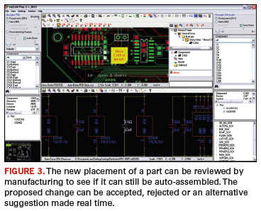
First, let’s look at some decisions during design that could make the difference between a successful product and one that misses revenue goals. One of these involves choosing components early and throughout ECOs (engineering change orders) in the design process. The choice of the wrong component (even though functionally correct) could mean an increase in product cost (high reliability and an expensive part into a consumer product). Another example is a part that requires manual versus automatic assembly, again increasing the product cost (FIGURE 3). Yet another is the ability to obtain enough parts to support your production volume.

The way to prevent these situations involves two areas requiring electronic design solution capabilities. First is the ability to produce work-in-progress BOMs and communicate those to the target procurement and manufacturing organizations. These should be produced as soon as the schematic is somewhat final and before layout begins. Given the BOMs, procurement and manufacturing can identify any potential problems.
Throughout the design process, ECOs requiring the change of parts or their locations is a common occurrence. Instead of producing another complete BOM, communicating just the change electronically can save time and money. A collaboration tool that communicates the proposed design change electronically through a user-friendly viewer and provides the capability for manufacturing and procurement to review the proposal and either accept or reject it, real time, can achieve the required results.
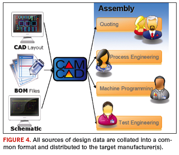
When it comes time to transfer the design into manufacturing, it can be a daunting task if the designer is required to understand all of the target manufacturer’s machine specific format and process steps. Here, the PCB design tools suppliers can provide the efficient bridge to manufacturing and reduce the pain of the designer. The designer can use a tool that takes all of the required design data and translates it into a common format (FIGURE 4). This common data can then be accepted by the target manufacturer(s) and automatically customized to their exact needs.

Design Everywhere
As we look at the typical large enterprise today, it often has its design resources dispersed at various locations around the country or around the world. As the company strives to meet its basic business goals of getting a competitive product to market faster with lower development costs, it needs to leverage these design resources in the most efficient manner. This involves not only the electronic designers, but all of the engineering disciplines required in the design and delivery process. These disciplines include but are not limited to the numerous ECAD disciplines (IC, FPGA, engineering, layout); numerous technologies (RF, analog, digital); MCAD, manufacturing engineering (such as test); and QA. The key is collaboration. How do you create an environment where all of these disciplines can collaborate on the same design in the most efficient manner?
Collaboration
Let’s begin with a look at the ECAD environment. How can you get multiple layout designers to work simultaneously on the same design, without partitioning, even if those designers are dispersed at different locations or around the world? This could be important in two situations. First, if you had a large digital board where applying multiple designers in parallel (versus serial in multiple shifts) could reduce your design cycle time. Secondly, if you have a mixed-technology board (RF, analog, digital) where you have experts either at the same location or again spread around the world. In this situation, not only are you changing a serial process into a parallel one, but you are also giving designers the opportunity to design their part in the context of the rest of the PCB, thus avoiding redesign cycles.
Design tool technology exists to accomplish these goals. Recently, design clients connected over a LAN or WAN, which enabled simultaneous edit to the same PCB, updating of a common database and letting the designers view the edits of the others real time. Through collaboration, users of this technology are experiencing up to a 70% reduction in design cycle times.
ECAD – MCAD Collaboration
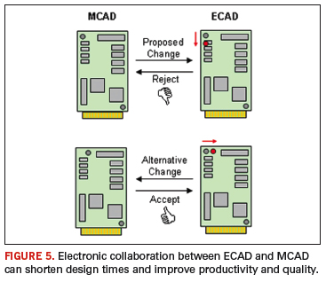
Extending collaboration into other disciplines beyond electronic design can also make a big difference in product development efficiency. An example is to create a collaboration environment where ECAD and MCAD designers communicate during the design process electronically versus via paper (FIGURE 5). The typical method of paper communication of proposed changes, either a proposal from the ECAD engineer or the MCAD designer for a change, is long, cumbersome and error prone. By implementing collaboration tools where:

- A change is proposed.
- That change is communicated to the other discipline electronically.
- The engineer has the opportunity to view the proposal in a familiar environment (viewed in a typical PCB layout tool or mechanical 3D tool) and can test the complete design (e.g. for enclosure interference).
- To comment, offer a counter proposal or approve the change, and then have that communicated back to the proposing party.
- If accepted, to have the change reflected into the databases of both the ECAD and MCAD engineers.
It is important here to distinguish between true ECAD – MCAD collaboration and 3D viewing or data transfer. Database transfer via the older existing standard (IDF) has long been used to interface the entire PCB design or mechanical enclosure (initial board outline, holes, component placements, etc.) from the MCAD to ECAD (or vice versa) at the beginning and end of the design process, respectively. This method does not identify the incremental changes during the design process nor does it support a collaboration process of proposal and acceptance. Neither is collaboration merely 3D viewing of PCB design data in a mechanical enclosure. Subtle errors such as interference, thermal hot spots or stress can go undetected unless analyzed by a sophisticated mechanical design tool. True collaboration requires the ability for incremental proposals to be communicated. This allows each discipline the opportunity to view and experiment with the change in its own ECAD or MCAD environment. Each discipline can then accept, reject or counter propose the change. Database update follows.
Global Intellectual Property (IP) Management
With a company’s design resources spread around the world, it is important that IP (component libraries, design constraints and intent, work-in-progress design data, design reuse data, best practices work flow, etc.) be easily created, protected and accessed by designers and manufacturing. This cannot be accomplished without sophisticated ECAD design flows supported with infrastructure capabilities on a worldwide basis. This type of infrastructure requires a significant investment by the company to build and maintain.
Also, the question might be: “Can a company’s ERP, PLM or CIS systems suffice to provide the IP management capability for the electronic designer?” The answer is “maybe,” given a large investment in customization and interfaces. However, the most efficient way to provide the designer with speed and access is to have a system and data that “are a mouse click away” by storing all of the IP in the design tool’s native formats. What is required though is that the ECAD design management system (DMS) is bi-directionally integrated with the company’s ERP, PLM and CIS systems to accept and provide data.
Globalization is a Challenge
Globalization is not coming; it is here and here to stay. For an electronics company to meet its driving business goals of producing the most competitive product faster and at reduced development costs, it must learn to leverage globalization instead of fighting it. EDA vendors can provide design systems that support many of the capabilities needed to capitalize on these resources and compete on a global basis, but some changes must also come in the company’s organizational structures and product development processes. PCD&F
John Isaac is director of market development for Montor Graphics Systems Design Division and can be reached at This email address is being protected from spambots. You need JavaScript enabled to view it..


