At PCB East, bi-directional communication was more than a
catch-phrase.
PCB East came to the Midwest last month for the first time. The show,
in its 13th year, blew into the Windy City, arriving at this new
location at a new time of year. Previously occurring in the fall, PCB
East has now been moved to the spring, changing positions with PCB
West, which rotates to Santa Clara in September.
The conference offered a number of new classes, and returned many
popular topics and speakers. Some topics new to
PCB East included; PCB
Design Using Metric Systems, taught by Andy Kowalewski, SyChip, If You
Can Make It, They Can Fake It: Counterfeit Parts and China, taught by
David Ackerman, Ackerman-USA and Death of a PCB Salesman, taught by
Greg Papandrew, Bare Broad Group. These classes are part of the FREE
Tuesday program, a popular
PCB East/West feature that coincides with
the opening of the two-day exhibition.
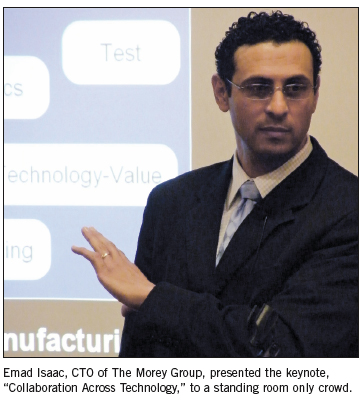
This year’s keynote was delivered by Emad Isaac to a standing
room-only audience. Isaac spoke of the importance of collaboration
across the electronics supply chain and specifically between design and
manufacturing. Isaac, CTO of The Morey Corp., explained how the
company, a $100 million EMS/ODM company that specializes in the design
and build of industrial controllers and telematics, actively identifies
potential design problems and communicates them across the supply chain
to continuously improve the manufacturing process.

In his talk, Isaac noted Morey performs design and assembly of products
used in heavy industrial machinery, and that the printed circuit board
is an integral connection between the two domains of design and
assembly that Morey internally controls.
He highlighted problems that come when information is not properly
communicated. “We don’t design PCBs with voids, but
sometimes we get them,” he said. When there’s a
break down,
Morey then works with suppliers to ensure that the requirements have
completely communicated.
For example, it is common practice to remove non-functional pads on the
outer layers of a design. But in one instance, the ODM designers had
called for landing pads to support the housing attachment. They were
not identified as having a special purpose. The layout designer saw
them as non-functional pads and, following common industry practices,
removed them. The result was an unusable PCB, a re-spin and a delay to
market, all costly to the project and all avoidable with better
communication along the supply chain.
According to Isaac, the new product development process involves
intellectual and practical components. Design is intellectual, and
manufacturing, practical. The need to collaborate between these
disciplines is critical to the success (or failure) of a program. The
better the communication, the more it involves all aspects of the
business, beginning with leadership, sales and the customer on the
intellectual side and including practical components such as
manufacturing, QA and procurement on the business side, the project
will be.
The presentation was illustrated by examples of DfM / DfT. According to
Isaac, pushing these validation tools to the beginning of the design
process reduces the number of re-spins and improves quality. Yet
quality is not the same thing as reliability, Isaac was careful to
point out. Quality focuses on the process, while reliability is related
to the testing.
For Morey, assembled board testing is critical. The use of HALT
(Highly-Accelerated Life Test) provides detailed information on product
long-term reliability. Systems supplied by Morey are designed for
20-year lives, in harsh environments, so knowing that the product will
pass “the shake and bake test” associated with the
HALT
protocol is important. Identifying and then communicating the cause of
a failure, providing appropriate feedback to the appropriate parties so
that the design and PCB fab process can be adjusted, completes the
loop.
Creating an environment that encourages communication across different
departments, technology areas and the supply chain is critical for
integration of key enabling technologies. According to Isaac,
“Any successful program starts with steady, honest, and
timely
information flowing bi-directionally.” It was evident from
the
discussions that collaboration is certainly at the core of this
company’s success.

Next-Gen Design Tools
During the conference, key PCB design tools vendors talked about the
challenges facing designers and potentially disruptive technologies on
the horizon. The connecting themes of collaboration, convergence,
co-design, communication – the 4 Cs – ran through
each
presentation.
Nikola Kontic of Zuken brought forward the importance of putting 3-D
design tools to the front end of the design process where the product
planning first interfaces with system-level conceptual design. He also
talked about changes occurring in the EU related to low power design.
Dr. How-Siang Yap of Agilent EEsof EDA talked about mixed-technology RF
products and tools that will enable co-design of the PCB, package and
IC. This approach will offer opportunities to optimize cost, size and
performance of electronic systems and is much needed today to meet
economic and time-to-market constraints.
Josh Moore of Cadence commented that seamless integration is critical
in electronics design becuase of the increased complexity. Designs have
a higher-level abstraction, requiring advanced automation techniques.
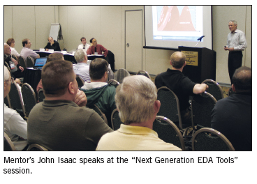
Mentor’s John Isaac talked about the need for continuous,
incremental improvements to the design process in addition to the
occasional major technology leap. To deliver these types of advances,
the industry needs to get better at collaborating and breaking down
barriers between disciplines.
There were more than a few revelations. When asked when simulation
tools for ground return modeling would be available, it was revealed
the capability exists in a new Agilent / Mentor tool. The session
served the dual purpose of enlightening designers on current tools
while allowing them to voice opinions about specific immediate needs.
‘Jam-Packed’ Conference
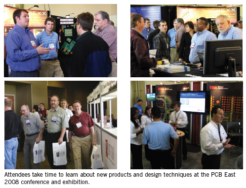
The one and one-half day exhibition featured products and services for
PCB design and fabrication. Fabricators like Dynamic & Proto
Circuits and Sierra Circuits showcased PCB, layout and engineering
services. Design tool suppliers including EMA Design Automation,
DownStream Technologies, Mentor Graphics and Intercept Technology
provided hands-on test-drives for prospective designers. Laminate
suppliers Rogers and DuPont featured new products for high-speed, RoHS
and embedded capacitance applications. For more information go to
pcdandf.com/cms/content/category/17/217/216/.

The
PCB East attendees had the opportunity to meet notable authors on
the show floor on Tuesday afternoon. Charles Pfeil of Mentor, a
conference speaker and columnist for Printed Circuit Design and Fab,
distributed signed copies of his recently released book, BGA Breakout
and Routing. Ralph Morrison, another speaker at
PCB East, presented,
Grounding and Shielding – Circuits and Interference, 5th
Edition.
Clyde F. Coombs talked about updates to the seminal, The Printed
Circuits Handbook, 6th Edition.
The
PCB East conference program was jam-packed with technical content.
The five-day program included over 40 topics. The two-day, full day and
one-half day courses and workshops where geared toward educating
designers in topics like high-speed, EMI and crosstalk, RF/microwave
design, PCB layout, HDI techniques and embedded passive design.
Over 65% of the program this year was new. Some of the highlights
included a half-day seminar titled, Design Principles for BGA, CSP and
3-D Package Technologies, taught by Vern Solberg. Solberg discussed the
design and manufacturing changes needed to address new finer-pitch ICs.
The seminar compared different commonly used packaging technologies.
Because of the density associated with these miniatures IC packages,
optimized design layout, land pattern geometry refinement and quality
substrate materials are critical to manufacturing efficiency and
product reliability.
Another timely workshop, Power System Design in High-Speed PCBs, was
taught by Rick Hartley, L-3 Communications. Hartley discussed
optimization of power system design (PSD) including the major
components of the power bus, the power distribution path, medium- and
high-frequency decoupling concerns, the importance of IC pin
assignments and the performance of power/ground planes. He covered
decoupling placement, real performance of capacitors, how much
decoupling is enough, why to use one value of capacitor versus another,
anti-resonant peaks and the importance of board stack-up in PSD.
It all added up to an educationally packed week. If you missed PCB
East, you can join us at
PCB West, September 14 – 19, 2008,
at
the Marriot, Santa Clara, CA. Don’t miss the opportunity to
network with your peers and learn some new skills.
PCD&F


