Maintaining the electroless copper process chemistry within recommended range can alleviate many common plating problems.
We
devoted the last several columns to voids and holewall pullaway. Before
moving on to discuss other defects, this edition will discuss resin
recession and finish with a case study on Holewall Pullaway (HWPA).
While they are two unrelated issues – one is a defect and the other is
not – both will receive appropriate discussion.
Resin
recession is primarily a material issue, not a plating/metallization
defect. On casual inspection, resin recession can be, and often is,
confused with HWPA. Resin shrinks during solder shock and other thermal
excursions, and resin that is not completely cured will be more prone
to shrinkage.
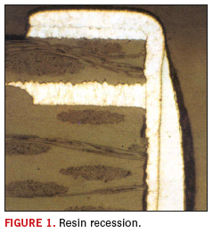
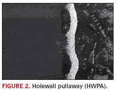
An example of resin recession is shown in Figure 1, and holewall pullaway in Figure 2.
One way to determine the difference is to look carefully at a
cross-section. In Figure 1, the plated copper edge is very straight,
and the resin is pulled back, indicating resin recession. In Figure 2,
one can see that the plated copper vertical sidewall is “bowed
outward.” The bowed copper is often seen as minor “blisters” or areas
where the copper has lost adhesion.


Resin
recession is often seen with under cured laminate. To check the degree
of cure, you can use thermal mechanical analysis or differential
scanning calorimetry. Undercured material will shrink or recede during
thermal excursions.
Depending on the type of
chemistry employed for desmear, certain material combinations can
exaggerate the degree of resin recession. If the solvent used prior to
permanganate is overly aggressive with respect to its penetration into
the resin, recession will be evident. If using a 100% organic solvent
for pre-conditioning, consider a different solvent system or one with a
reduced concentration to minimize penetration.
A PCB
fabricator recently reported a an increase of sporadic holewall
pullaway. The defect was exhibited in both small and large diameter
vias in standard FR-4 material. Defects were seen on multilayer designs
of 6 to 8 layers. For the past two years, a standard EDTA based
electroless copper (medium deposition type) was employed. The process
was designed to deposit 50 to 60 microinches of copper in 30 minutes.
Solution operating temperature was specified to be 75 to 85 degrees F.
The
operators were interviewed and suggested “nothing had changed” in the
process operation, yet visual inspection of some panels showed a
noticeably darker color to the plated copper on some product. In
addition, weight gain measurements yielded information that indicated
that occasionally, deposits as high as 90 to 100 microinches of copper
were recorded. Interestingly, the operators were not concerned with
this discrepancy, but solder floating several coupons from these
overplated boards showed a high level of HWPA. The main cause is quite
simple – the electroless copper deposit was deposited in a stressed
condition. Remember, this particular electroless copper process is
formulated to deposit 50 to 60 microinches in 30 minutes, not 90 to 100
microinches in the same time period. Keep in mind that when the
electroless copper process is operated outside of normal operating
parameters, problems can happen.
Now let’s get to
the root cause of the problem. Often it’s in the details. The
electroless copper solution was maintained with a single channel
controller that monitored the copper content in the working solution.
Based on the copper analysis, the other chemicals were replenished in
the standard proportion required to maintain the process in the working
range. This means that the sodium hydroxide content was added based on
the copper that was required in the solution.
Unfortunately,
the sensor for the copper was not calibrated properly. Thus, the
controller thought it was seeing a lower level of copper than what was
really in solution. In reaction to the incorrectly measured, low copper
levels, the controller called for the addition of copper and sodium
hydroxide in amounts that where much higher than the electroless copper
process needed. The higher than required levels of hydroxide drove the
deposition rate beyond the designed 50 to 60 microinches, resulting in
the stressed, heavy copper deposit.
Remember, any
process change that can lead to a greater than normal deposition rate
can cause holewall pullaway. All chemistries should be operated and
maintained according to the manufacturers’ recommendations. PCD&F
Michael Carano is vice president for OM Group Inc. and can be reached at This email address is being protected from spambots. You need JavaScript enabled to view it..


