Next generation ASIC and FPGA packages with 0.8-mm pitch and over
2,000 pins will require the use of HDI to accomplish BGA routing.
This
is the second in a series of articles on BGA routing methods. My goal
is to highlight routing problems associated with large pin-count BGAs,
and provide the PCB designer with effective techniques that enable
higher route density and reduction of layer count.
The
good news is that BGA technology enables high pin-count FPGAs, ASICs
and connectors packaged with a very high density array of pins. The bad
news is that finer pin-pitches and increased pin-counts are making
these devices increasingly difficult to route. The requirement to
miniaturize while increasing functionality is the most significant
constant driving change in our industry. Fortunately, it keeps skilled
PCB designers (and former designers like me working for software
vendors) employed!
High Pin Counts
The
current crop of BGAs with less than a 1-mm pitch are not yet pushing
high pin-count and as such they can be fairly easily routed. Very high
pin-counts can be found in currently used 1-mm pitch packages, and this
pitch will be decreasing to 0.8 mm in the coming years.
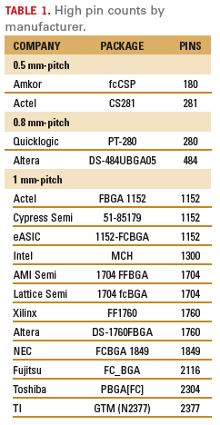
In Table 1,
the highest pin-counts for various FPGA and ASIC packages are listed.
Note: Even though I was able to find a data sheet for the highest
pin-count packages, I am not certain if they are actually in
production. If anyone can provide information for actual devices with
very high pin-counts, I will add them to this chart in a future
article.

Impact on Routing, Performance and Cost
Since
the pin-counts on 0.8-mm pitch BGAs are still reasonably low, the
routing task is not too difficult. However there are still some design
requirements to be considered:
- Differential pairs. Unless
the design rules in the device area are very small, or innovative via
patterns are used (to be described in a later article) then the diff
pairs must be split. Since these packages are still quite small, the
split distance may not affect signal integrity. You also need to
determine if the impedance discontinuity could have an impact. For 1-mm
pitch BGAs, I consider a pin-count over 1,500 to be the first threshold
for routing difficulty. In the context of laminated FR-4 boards with
through-vias, these are some of the potential problems:
- Layer count. The
large number of pins could require additional layers simply to breakout
the device. If you have multiple uses of BGAs with more than 1,500
pins, then the route density will require more routing layers. Layer
counts over 28 need thinner FR-4 dielectrics and de-lamination can
occur at lead-free assembly temperatures.
- Via aspect ratio.
Maintaining high fabrication yields and long-term reliability requires
the via length-to-hole size ratio to be less than 10:1, preferably 8:1.
Boards with over 28 layers make it difficult to keep the through-via
size small enough to allow effective routing. As the via pad size
increases, it is more likely that diff pairs will have to be split
during the breakout as well.
- The “Catch 22” of circular dependencies.
High pin-counts dictate additional layers to route, additional layers
require a larger via hole and pad size, and larger vias then reduce
routing space forcing additional layers. Once caught in this cycle, the
best way out is to abandon through-vias and start using blind and
buried-vias or high density interconnect (HDI) with applied dielectrics
and microvias. BGA pin counts greater than 2,000 at a 1-mm pitch is a
tipping point, especially if you have multiple ICs on a single board,
as you might see in a network or emulation card. The layer count and
via aspect ratio problems with laminated FR-4 boards will be even more
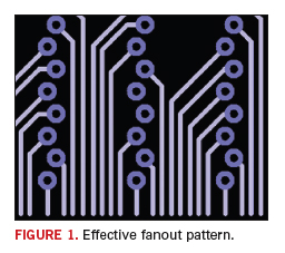
complex. When using blind and buried vias or HDI microvias, effective
fanout patterns can be used to increase route density from 24% to 36%
with a corresponding layer reduction. Figure 1 illustrates this, showing increased route density on the first inner layer of a design when using blind and buried vias.

Off-Matrix Ball Pads
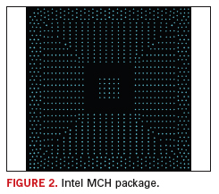
The Intel Memory Controller Hub (MCH) BGA package, which can have up to 1,300 pins, is worthy of special mention. Figure 2
shows how the pins are positioned off the standard matrix, making the
routing difficult. Depending on your design rules, this may require
routing with any-angle traces. This is a new package from Intel and
gives us a view into the future – BGA routing isn’t going to get easier
anytime soon. Fortunately, PCB design software continues to be enhanced
to keep pace with the evolving packaging methods.

The Near Future
In
order to increase functionality and continue to miniaturize, higher pin
count will be incorporated into smaller packages. I predict that within
the next three years we will see an ASIC or FPGA package at 0.8-mm
pitch with greater than 2,000 pins, and within five years, the use of
this kind of package will be common. This will be a paradigm shift for
PCB design because this type of device will require the use of HDI.
Upcoming BGA Bulletin articles will demonstrate how to apply HDI and
fanout patterns while fulfilling your performance and manufacturing
requirements. PCD&F
Charles Pfeil is a product marketing director for Mentor Graphics, Systems Design Division; This email address is being protected from spambots. You need JavaScript enabled to view it..


