Successful design/characterization of PCB high-speed interfaces frequently demand analyses of timing margins and jitter.
The digital signal integrity as a discipline1
came into existence in the 1960s, and three main signaling schemes have
since emerged. These signaling methods include common clock, source
synchronous and high-speed serial.
Many SI issues in
modern digital interfaces are caused by reflection, crosstalk,
attenuation, resonances, and power distribution noise. However, the
actual failure mechanism does not involve voltage waveforms (at input
of the receiver ICs), but a timing relationship1 between
those waveforms and the clock that samples the signal. It has been
observed that “ninety percent of signal integrity problems are timing
problems2.”
Several concepts and
mathematical formulae governing common clock and source synchronous
timing were described in previous columns3,4. One way to apply timing equations is by generating a spreadsheet to compute allowable worst (and best) case flight times5 and timing budgets. Figure 1 displays section of a timing spreadsheet created utilizing Microsoft Excel.

The
spreadsheet was generated to summarize the timing results for various
nets of a high-speed parallel bus. The column entries display net
names, driver reference designations (plus pin names), receiver
designations (and pin names), minimum and maximum rise times, minimum
and maximum flight times, setup and hold margins. For a bi-directional
bus, it is necessary to solve the min/max flight times for each signal
direction. Such spreadsheets can readily indicate which nets have
failed setup or hold timing margins and hence require an improvement to
meet timing requirements.
Timing budgets may be also presented in table format6.
Several programs are available to aid system timing analysis and
verification. Such software include Timing Designer from Forte Design
Systems, Timing Diagrammer Pro from Synaptic CAD, Inc, TimingTool (a
free, intranet-based timingtool.com timing diagram editor) and Tau7.
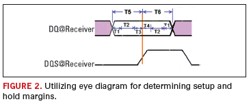
Eye diagrams also offer an effective means for ascertaining the setup / hold margins for source synchronous buses8, centering clock transitions in the middle of the data eye2 and for deriving timing equations4.
Figure 2
illustrates how setup and hold margins for a source synchronous signals
may be determined via an eye diagram. Here T1 represents timing margin,
T2 equals skew, T3 is setup time and T4 is hold time, T5 is “valid
before time” (i.e., the time before the strobe occurs when the data
signal will be valid).

T6 is “valid after time” (i.e., the time after the strobe occurs for which the data is still valid).
When
timing failures (or signal quality violations) are detected for a
signal net, the signal performance may improved by altering/enhancing
termination, topology9, 10 or technology (sometimes called the “the three Ts”).
As clock frequencies increase, timing becomes more critical11.
Timing margins for parallel bus architectures diminish and signal
flight times (propagation delays) are reduced to picoseconds. Because
such tight tolerances are often not feasible to obtain, the serial data
bus architectures have emerged and gained popularity for the fastest
systems.
Eye diagrams provide a preferred/intuitive
means for timing analysis of high-speed differential serial links (with
embedded clocks). Eye height is the eye opening in the amplitude domain
and eye width relates to signal timing and jitter12. Eye
masks are applied to more easily determine pass/fail conditions. Eye
width and height are bounded by a mask, and any violation of the mask
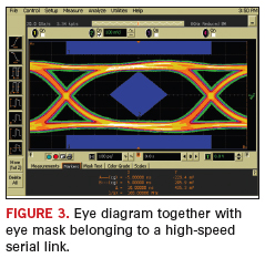
boundaries can indicate non-compliance12. An example of eye diagram together with eye mask (shown in blue) is provided by Figure 3. It displays signal captured (at the receiver end) for a 1.5 Gb/s Serial ATA (SATA) bus.

Figure
3 depicts a sufficiently open eye. When the eye is closed, there are
various techniques such as pre-emphasis or equalization13 which may be applied to open the eye.
Pseudo-random binary sequence (PRBS) patterns14
are frequently used as stimulus (to the channel) to generate eye
contours. PRBS is a data pattern that attempts to replicate truly
random data yet it is completely deterministic. PRBS patterns have
length of [(2^N)-1], such as [(2^7) – 1] = 127 bits.
Each
signaling standard (e.g. SATA, PCI Express, XAUI, HDMI, etc.) specifies
how to capture data for eye measurements (including clock recovery
method) and the masks that ascertain compliance or non-compliance12.
Many high-speed serial links incorporate 8b/10b encoding12 to guarantee minimum transition of data (to aid receiver recover clock) and apply scrambler to reduce EMI.
Certain
test equipment such as Agilent Infiniium DSO81204A (12 GHz 40 GSa/s)
allow jitter measurements on ultra-fast serial signals and can display
total jitter, random jitter, deterministic jitter, data-dependent
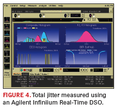
jitter, as well as pattern and periodic jitter. An example is
illustrated by Figure 4, which decomposes jitter into
subcomponents to facilitate debugging. Figure 4 also displays histogram
and bit error rate (BER) bathtub curves. Such displays are useful for
quickly correlating15 multiple answers, detecting Intersysmbol interference (ISI), and knowing whether the device meets the standard.

ISI can be caused by transmission line losses (which degrade signal rise time) and lead to degradation of the eye diagram13. BER is an important metric16
for quantifying the performance of high-speed serial architectures. The
BER and jitter analyses/testing have become a necessity to assure
performance requirements for high-speed serial links, particularly due
to the increasing data speeds. PCD&F
Dr. Abe (Abbas) Riazi is a senior staff electronic scientist with ServerWorks (a Broadcom Company) in Santa Clara, CA.
ACKNOWLEDGEMENTS
Special thanks to Richard Kuo for reviewing the manuscript and providing valuable comments.
REFERENCES
1. Greg Edlund, ”Timing Analysis and Simulation for Signal Integrity Engineers”, Prentice Hall, 2007, P.2, PP. 13-14.
2. Jim Peterson, “Timing Numbers from ICX - What Do We Do With Them?”
Mentor Graphics International User Conference May 2-5, 2006.
3. Abe Riazi, “ Timing Analysis Principles for Digital PCBs, Part 2”, Printed Circuit Design & Manufacture, June 2006, PP. 20-21.
4. Abe Riazi, “ Timing Analysis Principles for Digital PCBs, Part 3”, Printed Circuit Design & Manufacture, August 2006, PP. 16-17.
5. Tod Westerhoff, “Closing the loop between timing analysis and signal integrity“, Cadence Online Seminar, August 28, 2000.
6. “DDR2 Design Guide For Two-DIMM Systems” Micron Technical Note, TN-47-01.
7. Tom Granberg, “Handbook of Digital Techniques for High-Speed Design“, Prentice Hall, 2004“ PP. 583-586.
8. Stephen H. Hall, Garrett W. Hall, James A. McCall, “High-Speed
Digital Design, A Handbook of Interconnect Theory and Design Practices,
“John Wiley and Sons Inc., 2000, PP. 186-190.
9. Bill Hargin, “Managing Signal Quality”, Xcell Journal, Second Quarter, 2005.
10. Abe Riazi, “Signal Quality Assessment”, Printed Circuit Design & Manufacture, June 2007. PP. 16-17
11. Roy G. Leventhal and Lynne Green, “Semiconductor Modeling For
Simulating Signal, Power, and Electromagnetic Integrity”, Springer,
2006, P. 30.
12. “The Basics of Serial Data Compliance and Validation Measurements”, Tektronix.
13. Eric Bogatin, Signal Integrity – Simplified, Prentice Hall, 2004, PP. 333-335, PP. 398-399.
14. Min Wang, Henri Maramis, Donald Telian, Kevin Chung “New Techniques
for Designing and Analyzing Multi-GigaHertz Serial Links”, DesignConn
2005.
15. “Agilent 86100C Infiniium DCA-J, the fastest way to the right answer”, Agilent Technologies.
16. Mike P. Li, and Dennis Petrich, “Characterization and Production
Testing At 3.2-5.0 GB/s for PCI Express II and FB DIMM”, 2006 Wavecrest
Corp.


