A coordinated design methodology fine-tunes chip-to-package PCB layout and routing.
When routing a ball grid array style package on a printed circuit board, have you ever wondered what the package designers were thinking when they came up with the pattern and pin assignments? Was there any consideration at all to the impact on the PCB? In most cases the answer is yes, but there was probably little the package designer could reasonably do to mitigate connectivity issues originating from the chip-level layout.
In some ways, the role of packaging has changed little over the past two decades. It still serves as the mechanical enclosure, manufacturing form factor, and thermal conduit for the silicon it encompasses. However, its signal and power delivery role is what has significant impact on the PCB layout. This is driven by the sheer number of signals moving through the package, along with decreasing noise margins and supply voltages. Today’s BGA-style packages have a significant impact on PCB layer count, route complexity and cost. Efficient BGA net assignment and patterning of power and ground pins can make the difference between a four- and a six-layer PCB.
Traditional methodology for chip-package-board design has been a serial top-down flow where the chip drives package connectivity and, in turn, the package drives board connectivity. While not ideal, the approach worked when the largest device on a PCB was still well under 1,000 pins and the matrix was three to four rows deep. With more functional integration taking place at the chip- and package-level, package pin counts continue to grow to a point where several thousand pin packages will not be uncommon.
To address these growing challenges, companies have moved to a more coordinated approach with emphasis on early planning between chip, package and board.
However, this is limited by use of separate implementation tools and databases: one for the chip, a second for the package, and a third for the board. As a result, most collaboration is done using spreadsheets to communicate pin assignments and plan interfaces. While a step in the right direction, it’s still a less-than-optimal solution. Spreadsheets are snapshots of static data that do little to facilitate real-time planning or improve efficiency, nor do they scale well with the increasing pin count and complexity.
In early generations of memory interfaces, the primary concern was efficient routing using the least amount of route resources. While still an objective, there’s now the added challenge of ensuring proper electrical performance and power delivery. In the past, if a signal meandered around pins or had a little extra length, there was little consequence due to liberal timing budgets and greater immunity to noise from the power system. The latest generation of multi-gigabit parallel bus interfaces like DDR3 or DDR4 has significantly smaller voltage swings than previous generations, leaving little tolerance for inefficient routing. Implementing these interfaces requires close coordination between chip, package and PCB, starting with chip-level macro and I/O pad ring placement, across package pin assignments and into board-level component placement.
Coordinated Design Methodology
Most companies and their engineers recognize the value of a coordinated design methodology across chip, package and board, but face both technical and non-technical obstacles to fully realize the benefit. It doesn’t make much sense when a packaging team produces an initial bump pattern and I/O pad ring placement only to have the IC team discard it and recreate the results because of the data format. Seems crazy, but it happens more often than most think. While the data format was an issue, the behavior has more to do with the silo culture found in some companies where design remains an over-the-wall process. Within their respective silos, groups are too consumed with tasks at hand to recognize a need to change. A tipping point is fast approaching, driven by package pin counts and high-speed interfaces where increased effort and manpower alone will not be enough, unless accompanied by a change in culture and methodology.
Communications across geographically dispersed design teams or with outsourced semiconductor assembly and test (OSAT) companies for packaging must factor into a coordinated design methodology. Most fabless semiconductor companies rely on OSATs for packaging and have a mechanism to provide initial die data – typically in some form of a spreadsheet. As the number of constraints associated with high-speed interfaces continues to grow in quantity and sophistication, this communication and exchange mechanism must adapt. It must be capable of communicating flexibility in some areas, i.e., pin swapping, while providing clear guidance and route intent in others. It must facilitate bidirectional communication, enabling the OSAT to communicate changes or recommendations back to the semiconductor company.
Driven by pin count and interface complexity, it’s clear a methodology change is in order to provide visibility and consideration of the PCB during chip-level floor planning and awareness of how decisions made early on impact downstream performance and cost. Considering where key board-level components and connectors are placed relative to a BGA-style package can greatly influence cross-fabric elements like package ball pad assignment and flip-chip bump configurations.
‘Multi-fabric’ planning. Coordinated chip, package and board planning is more than a change in methodology. It necessitates new tools and flows capable of delivering a multi-fabric view of the system hierarchy, while providing simultaneous access to domain-specific data like macro placement, I/O pad ring devices, bump patterns, ball pad assignments, and placement of critical PCB components and connectors.
This unique class of planning tool requires innovative functionality to manage and manipulate a range of multi-fabric data at various stages of completeness, and adapt as portions of the design become less abstract during the planning process. Integration and usability are crucial to minimize disruption, while still providing fast ramp-up for casual users. The major components of multi-fabric planning include system definition, bump/ball pad patterning, connectivity planning and net assignment, and interface planning.
A fundamental aspect of multi-fabric planning is the ability to quickly make placement and net changes in one fabric and immediately see the impact on adjacent fabrics. This requires an environment capable of uniting design data of various sources and formats for the purpose of planning, then communicating the data back to the respective implementation tools for completion.
One of the first steps of multi-fabric planning is establishing the physical relationship between the chip, package and board. In other words, establishing the full system representation. This is accomplished using hierarchy management to establish and manage the relationships among the fabrics (Figure 1). It enables representations of the complete system from the chip-level to the PCB, while maintaining the integrity of individual design fabrics. Most every aspect of planning and exploration will reference the hierarchy before performing a given task.

Bottom-up planning from the PCB. Consider the scenario of incorporating an advanced package onto a PCB that targets a consumer product for which cost and performance are the primary drivers. While device placement and assignment decisions made solely in the context of the chip may yield the ideal chip-level design, they could ultimately result in missing the cost and performance targets for the end product. In such a top-down system flow, the chip-level placement dictates the bump and ball assignments in the downstream fabrics. This could result in excessive coupling in the high-speed memory interface and a needlessly complex escape routing scheme that requires additional layers in the package and PCB substrates.
A more cohesive approach utilizing multi-fabric planning would establish an initial ball pad assignment that considers the critical components, routing, and layer constraints of the PCB, and then propagates it into the package to influence the flip-chip bump pattern for the die. The flip-chip bump pattern, in turn, would influence die-level I/O pad ring device placement and redistribution layer (RDL) routing. While it’s unrealistic to drive the system entirely from the bottom-up, factoring in aspects of the PCB and package during early planning is a necessity to achieve product cost and performance targets.
Interface definition and optimization. Just as spreadsheets were the old way of communicating pin assignments, tools like PowerPoint or Visio were the choice for interface planning or as means of communicating design intent. Used to sketch out and visualize a route plan, they quickly lose usefulness as the number and complexity of interfaces and signals increase within a design.
Today’s high-speed interfaces require careful planning across multiple devices and fabrics to ensure proper performance. Interface planning helps drive pin assignments, flow and location of major busses, and evaluates interaction with other interfaces and signals within the system. It provides flexibility to work at a coarse level to establish initial placement, then refine down to the individual byte lanes as a plan emerges. Interface planning is made up of three major steps: interface definition, floor-planning and flow planning.
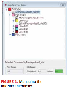
Defining an interface creates the logical hierarchy starting with the overall interface, i.e. PCIe, continuing down to the individual ports (Figure 2). For example, a PCIe interface may contain two major banks comprised of four-byte lanes each, with each lane containing four differential pairs comprised of two ports. An interface definition spans multiple fabrics and provides the management mechanism for floor-planning and bundling. The definition may be done independently of net list to facilitate early exploration with the ability to map in the nets at a later stage (Figure 3).

Floor-planning an interface takes place within each individual fabric to establish a target set of pins. Within this group, some pins will be allocated for signal assignment, while others will be reserved for power or ground. Their relative locations may be established to ensure a sufficient signal-power-ground ratio and proper return paths for the signals. Floor-plans from the respective fabrics are then associated with an interface, adding the physical definition to what was previously a logical representation.
The last step is flow planning using bundles to define the relative path of an interface within a fabric, as well as defining connectivity between fabrics. A bundle is a mechanism to convey connectivity using the floorplan from one fabric to drive assignments to a floorplan in an adjacent fabric. Consider a scenario with fixed DDR memory on the PCB connecting to a BGA package. A bundle would be used to represent the proposed route path originating from the board-level memory to a floorplan of pins on the BGA (Figure 4). Functionality within the bundle editor would optimize pin assignments to the floorplan on the BGA, as well as evaluate the breakout route feasibility from the ball pads. Bundles also help visualize the size of the associated bus, as well as the respective layer it resides on.

Ideally, interface definitions and bundle paths defined during multi-fabric planning pass directly into the implementation tools, helping accelerate the design process. This also becomes a highly valuable mechanism to communicate design intent within an organization, as well as with external design resources.
Validating assignments with package auto-routing. While a fabless semiconductor company may take the lead on multi-fabric planning, it’s likely an OSAT will be responsible for the detailed package implementation. However, OSATs can also serve as a valuable resource during the planning process, provided there’s an efficient communication and data exchange mechanism. Once the semiconductor company has defined pin assignments and an interface plan, the data can be shared with the OSAT – ideally using a direct database exchange to preserve interface groups and constraints.
Historically, the turnaround time from OSATs was in the two- to three-week range for feasibility planning, with that number growing as the number of constraints and complexity increased. With packaging trends moving toward thousands of connections, and 50% to 75% of the nets having high-speed constraints, OSATs now recognize the need for greater automation to reduce their cycle-times and maintain competitiveness. Many are turning to new packaging-specific autorouting technology to address the high-speed constraints and geometrical challenges of advanced flip-chip packages. The speed and quality of this routing enable significantly faster turnaround, providing the capability to validate pin assignments and constraint compliance. This, coupled with direct database exchange, enables the OSATs to serve as a valuable planning resource.
High-speed interface implementation on the PCB. Once multi-fabric planning is used to establish the optimal package ball pad assignment in coordination with the PCB, the next challenge is implementing the high-speed interfaces at the board level. With increasing data rates and lower voltages translating into more constraints and complexity, design tools must provide innovative functionality to assist the designer in implementing high-performance interconnects. In some situations, complete automation (like autorouting) cannot provide satisfactory results and still enforce the number of diverse and sometime ambiguous constraints. Designers will require auto-interactive tools that enable them to apply their experience and intuition supported by semi-automatic route engines for efficient implementation of constraints and interconnects.
In the case of a DDR interface, numerous constraints define the structure and timing of the various byte lanes, differential-pairs, and strobes that make up the interface. Adhering to these constraints typically means an iterative process of trips between the design canvas and constraint management system to confirm that the actual routing meets the rules. As interfaces continue to grow in size and complexity, this has become a time-consuming process.
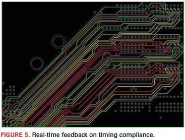
Some innovative design tools include functionality that provides a timing vision mode on the design canvas that uses color-coding of nets to indicate timing compliance. Color-coding dynamically updates during trace editing, with specific colors representing the necessary adjustments needed to bring a net into compliance: i.e., red = too long, yellow = too short, or green indicating compliance. Timing vision provides the designer real-time feedback as they’re editing without the need to constantly check the constraint manager.
Additional auto-interactive functions for delay and phase tuning allow the designer to tune signals or byte lanes. It’s based on the idea that the designer knows how to utilize the PCB design space more efficiently, while providing flexibility to tune signals in the order they think best. For example, differential pairs within a DDR interface require phase tuning and, unless those are properly addressed, it doesn’t matter how well you meet timing on the rest of the byte lane. In this scenario, auto-interactive phase tuning would be used to meet the static and dynamic phase requirements, followed by auto-interactive delay tuning on the byte lane or entire interface.
Given the reduced margins of error, methodologies must adapt to incorporate electrical performance assessment (EPA) into the design process. EPA enables designers to evaluate electrical quality and performance throughout the design process, helping avoid the backend analysis crunch – possibly jeopardizing product delivery. It utilizes extraction technology in a manner that provides actionable feedback to the designer, helping identify and avoid issues related to impedance discontinuities, timing, coupling or DC current density.
Summary
The trend toward greater functionality at the chip- or package-level will continue for the foreseeable future. A quick look in any industry publication will show a number of companies evaluating or using 3D-IC or interposer technologies to increase integration, which translates into higher pin counts and high-performance interfaces. Failure to properly plan and account for the PCB during chip floor-planning will result in a needlessly complex system that comes up short against performance and cost targets.
Multi-fabric planning that unifies chip, package and PCB to facilitate bottom-up planning is a more efficient path to product realization. It supports critical decision-making on issues that impact performance, complexity, and cost at a point in the design process when it’s the most practical and economical to affect change.
Kevin Rinebold is senior product marketing manager, IC packaging, SiP, and co-design solutions at Cadence (cadence.com); This email address is being protected from spambots. You need JavaScript enabled to view it..


