New tools allow concurrent creation of advanced stack dies, packages and PCBs.
In pursuit of feature-rich, light, compact products at a lower cost in less time, designers are increasingly creating complex multi-board products and using new packaging technologies to pack integrated circuits more closely together. Multi-board designs create new challenges such as planning and management of interconnects at the system level. The greater complexity of new packaging technologies means components need to be more tightly coordinated with one another so that pin assignments can be optimized for small size and minimum layer count substrates. Traditional 2D printed circuit board design systems are not well-suited to address these challenges because they are used to design one PCB at a time in isolation from the other PCBs within a product and also in isolation from the ICs, packages and enclosure.
A new generation of 3D multi-board product-level design tools manages multi-board placement in both 2D and 3D and enables co-design of the chip, package and board in a single environment. Multi-board design makes it possible to create and validate a design with any combination of system-on-chips (SoC), packages and PCBs as a complete system. Chip-package-board co-design enables designers to optimize routability via pin assignment, and I/O placement to
minimize layer counts between the package, chip and board. The new design methodology makes it possible to deliver more functional, higher performing and less expensive products to market in less time.
Multi-board design challenges. Despite the widespread and increasing use of multi-board designs, PCB design tools have continued to focus on working in 2D, one PCB at a time, with the electrical work done in 2D and then the 2D design exported to 3D mechanical design software where the boards are positioned and checked for interference. The limitation of this approach is that if a problem such as an interference is identified, it’s necessary to go back and forth between two different environments – PCB and mechanical design – to solve it. It is also awkward to perform a high-level design study, such as evaluating whether a two-board or three-board design is best and which blocks should be allocated to which board. This helps explain why an estimated 50% of complex products require at least one additional PCB fabrication to address electromechanical issues.
Interconnect management is also problematic using current design methods. In current generation tools the signal verification process for a multi-board design typically involves exporting pin lists that include net names for each board connector and correlating the net names to the master list of net names. In many cases it’s also necessary to manually verify each board connector’s signal name. With mechanical engineers and board designers working with disconnected systems it’s difficult, if not impossible, to intelligently manage connectivity and changes between boards. Using a spreadsheet or some other disconnected document to manage the large number of interconnects between the PCBs is time-consuming and prone to error.
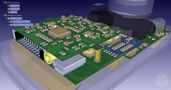
When mechanical engineers have inaccurate information on the electrical design, or electrical engineers have inaccurate information on the mechanical design, the result in many cases is batteries don’t fit; mounting screws create shorts against PCBs, and connectors don’t mate with packaging openings. Improper management can easily result in wasted product development time, scrapped boards and slipped schedules (FIGURE 1).

Figure 1. Multi-board design of three PCBs, along with their enclosure in 3D.
3D design challenges. New packaging technologies have proliferated to compensate for increasing silicon costs. Meanwhile, PCB technology has evolved with high-density interconnect PCBs, high-density packaging, embedded components and advanced I/O technology. The greater complexity of these new configurations is creating major challenges for packaging designers, as well as for the PCB and IC designers who must integrate the package into their own work. Traditionally, the PCB, the IC and the package are each designed in their own standalone 2D environment. PCB design software has been enhanced to address technology advancements with improvements in routing, constraint management, and signal and power integrity analysis. But these improvements have largely been limited in scope to the PCB design process.
With increasing functionality, tighter cost constraints, and the decreasing form factor of today’s products such as portables, wearables and the Internet of Things (IoT), components need to be tightly coordinated with one another so pin assignments can be optimized for small size and minimum layer count substrates. The overall goal is to align the board, package and chip so each signal follows the shortest possible path from the chip to the board, resulting in the fewest possible layers in the package. With the lack of tool integration, but increasing design requirements, engineers have reverted to workarounds such as using spreadsheets and generic office productivity tools to perform planning and feasibility studies and to define the tool interfaces and data transfer.

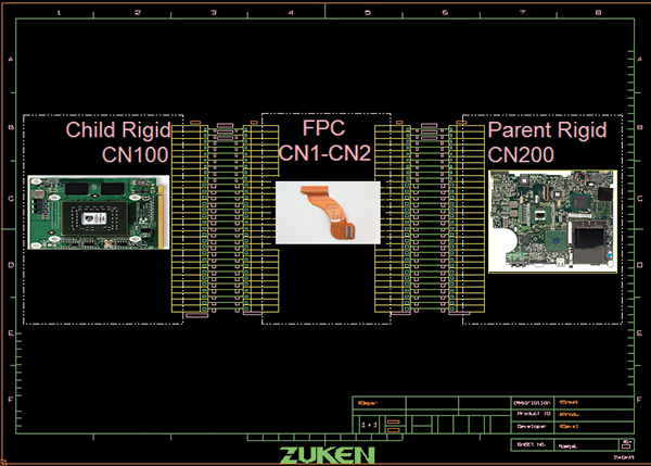
Figure 2. Product-level multi-board schematic.
3D design tools address multi-board design. A new generation of 3D multi-board, chip-package-board co-design tools addresses these challenges by providing an environment for system design that integrates 2D and 3D multi-board design, along with the chip and package. Designers can manage all the boards in the system in a single view to define the connections between them, highlight the signal across each entity and analyze the entire interconnect length.
The number, size, type and configuration of PCBs, along with alternative allocations of functions across them, can be evaluated collaboratively with the ability to make tradeoffs. Functional blocks can be assigned and moved between boards, and boards can be reshaped, added and subtracted as necessary. The 3D multi-board design tool can address signal continuity at the system level while simultaneously managing multiple PCBs’ interconnects and understanding board-to-board signal continuity.

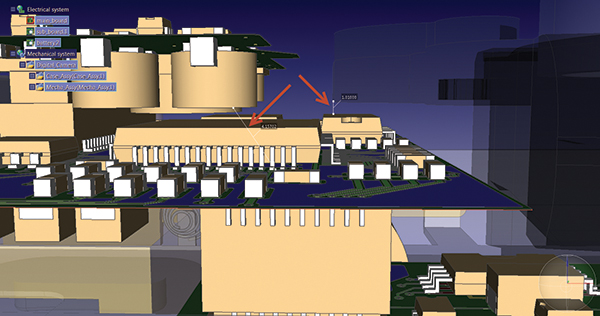
Figure 3. 3D clearance checking in the native ECAD tool.
PCB designers gain the ability to import the mechanical enclosure directly into the ECAD tool so they can get single or multi-board designs right the first time. 3D parametric libraries are shared between the ECAD and MCAD systems. During layout, users invoke a wizard to import the 3D enclosure model and specify all the associated PCBs. They then layout the PCBs with the enclosure in real-time, optimizing placement capacity and capturing interference violations earlier in the design process.
Electrical engineers can design to the true native 3D constraints as defined by mechanical engineers, while the latter in turn have access to the true 3D board design so they can accurately conduct interference checks during board layout. Electrical engineers can design multiple boards within a single model to ensure precise positioning of angles, shapes and cuts needed to avoid interference. Working with the exact product shape makes it possible to, for example, fit more functionality into a package that is curved to conform to interior styling than could be accomplished with an orthogonal approximation. 3D ECAD design enables more accurate alignment of connectors so they precisely fit openings on the enclosures.
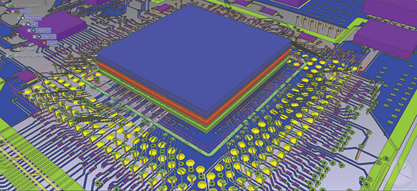
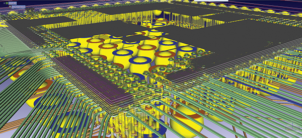
Chip-package-board co-design. By integrating planning and final design for PCBs, packages and ICs in a single view, the newest generation of tools makes it possible for engineers to conduct system-level co-design of the PCB, package and chip and optimize I/O placement, pin assignments, redistribution layer (RDL) routing, and bump and ball placements (FIGURE 4). The benefits are particularly great when working with non-traditional structures with routing complexity in both vertical directions such as package-on-package (PoP), system in package (SiP), chip-scale packaging and 3D-IC/3D packaging. The new tools also automate routing of the chip RDL and package escape, reducing pathfinding cycle time and making it possible to optimize die bump placement (FIGURE 5).

Figure 4. Co-design environment for chip, package and board in 3D.

Figure 5. Flip chip with redistribution layers in 3D.
Such tools allow all those working on the project to see their piece of the puzzle in the context of the full product, making it easier to optimize pin assignments and avoid connectivity errors. For example, package/IC bump assignment can be performed while viewing the effects on the ratsnest at the PCB level. The designer can observe the potential impact at the package and IC level of making automatic or interactive pin swaps at the board level to improve PCB routability. The pin swap operation is automatically communicated between the package and PCB databases, eliminating the need for CSV or other neutral files to communicate the change. Multiple engineers can work simultaneously on a single substrate because the tool enables engineers to lock the package design. If a designer needs to make a pin swap in a locked package design, he or she can send a notification that the other engineers can accept or reject as an ECO.
Simulation. The effects of changes from a signal integrity, power integrity or thermal point of view can be determined by performing multi-discipline, multi-physics analysis with tools from providers such as Keysight Technologies, ANSYS, AWR, CST and Synopsys. The co-design environment enables signal traceability across the complete system. Signal paths can be reviewed and analyzed as they cross design and component boundaries from drivers through the system interconnect to receivers. Intelligent and integrated schematic- or layout-based simulation environments support multiple design flows.
The new integrated 3D multi-board chip-package-board co-design environment makes it possible to holistically optimize the package, board and IC design to a greater degree than was possible in the past, with the end result being higher performance and lower manufacturing costs. Real-time 3D hierarchical design enables design teams to concurrently create combinations of advanced stack dies, packages and PCBs. With a native 2D and 3D architecture, designers can effectively co-design a chip, package and board to optimize I/Os at each level, embed components in the dielectric of a stack-up intelligently, and verify manufacturing rules in real-time. Next-generation tools manage multiple boards and their associated enclosures simultaneously and provide 3D clearance checking directly in the native electronic CAD tool.
Craig Armenti is senior technical marketing manager for PCB products at Zuken USA (zukenusa.com); This email address is being protected from spambots. You need JavaScript enabled to view it.. He is speaking at PCB West in September (pcbwest.com).


