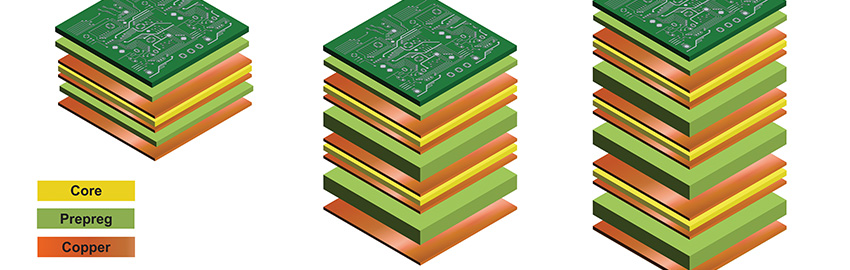
A printed circuit is an antenna for transmitting and receiving energy.
A raging fraternity party with thumping house music can be annoying as the morning hours approach. Noise suppression ordinances to the rescue! The partiers have two choices: quiet down or get shut down.
In that sense, the fraternity party is like building an electronic circuit. If our machines make too much “noise” in any part of the spectrum, it’s game over.
Just like kids can stop trampling everyone’s lawn and come inside, shut the doors, windows, shutters and even the fireplace flue, we can also contain unwanted spectral emissions. Left unchecked, a printed circuit is an antenna for transmitting and receiving energy from within and outside the board.
Even a well-designed PCB has compromises. Our goal is to be ready to react to spurious emissions that take us beyond the allowable threshold. We start with a power budget, and a noise floor, and our electronics must comply with those design criteria while meeting regulatory requirements.
As we bring different functions aboard, the problems in the near field multiply. We think of high-speed transmission lines as the focus of our EMI abatement efforts. They are seen as the cause of the problem, owing to their signal rise times or a harmonic of that momentary event.
To continue reading, please log in or register using the link in the upper right corner of the page.
Read more: The Art of Stifling Interference on a Printed Circuit Board Assembly
Quality is found in the design as well as the process.
Solder defects are inevitable. Reducing their risk is mandatory, especially if you’re aiming to make money as a result of operations. Machines are certainly not “almost human,” but they do go through seasonal changes and have moods. Without proper upkeep, they fall into disrepair. The goal in assembly is to dial in the thermal profile of the soldering equipment to minimize solder defects.
Footprint model accuracy is an enabler, but that work can be undone by improper routing and copper-flooding techniques. Placement too near the edge of the board where the temperature fluctuates to a greater degree can decrease yields through the soldering process. Tombstoning is one thing to watch for, but other dangers are present on the frontier.
The Goldilocks zone. Another defect can occur when one lead of a component is close to the edge while the other is farther inward. Wirewound resistors and inductors can become open circuits or more insidiously latent defects, where the wire pulls away from the lead only when there is a temperature rise or a mechanical shock to the system. Ceramic caps can actually crack when one lead solidifies before the other one.
To continue reading, please log in or register using the link in the upper right corner of the page.
Read more: Solderability is More than Selecting the Right Solder
They play an outsized role in continuous improvement.
Time was creating drawings meant using paper and a pencil. Can you imagine? The main variable was the type of so-called lead in the pencil. Even in those primitive times, it was necessary to agree on an overall language. The particulars that allowed the community to get its message across were determined by standards. Standards, in turn, were driven by the requirements of the equipment that archived and reproduced the drawings.
One of those pieces of equipment was microfilm. You might recall microfilm stores many drawings in a small space. Bringing those tiny pictures back to human-readable sizes would lose some of the sharpness of the data. Standards were set up so we could still make out the images and data with no doubt about what we saw.
Drafters would pencil-in the linework and run the pencil over the object lines again and again to ensure it was certain to come back from the photographic shrinkage. Text sizes and, importantly, space between characters, were a function of the size of the drawing. Smaller A and B size documents could use 0.125" minimum text height, while C-size formats and above required 0.140" letters and numbers. Minimum spacing between rows is half of the text height, so taller lettering gets more space.
To continue reading, please log in or register using the link in the upper right corner of the page.
Read more: Why Do We Have to Follow Drawing Standards?
What Charlie Brown can teach us about board design.
Not all boards are alike. In fact, no two are exactly the same. That’s kind of the point. We always do something that hasn’t been done before, or we wouldn’t be doing it. The best we can say is many boards share similarities. Just the same, someone in every organization wants to know when the one-off job will be completed.
Often, there is a predetermined schedule in which someone who has never drawn a trace decides when the PCB layout needs to be finished. Such a schedule is usually the result of market forces. It could be back-to-school, CES, or even (especially) a rocket launch date that drives the deadline. Still, it’s not unusual for stakeholders to ask your opinion about the estimated tape-out date.
Life in a service bureau or as an outside contractor. Service bureaus live or die by the accuracy of their bids. If their bid is too many hours, the customer will shop around. If the bid is too few, the designers end up eating that cost with overtime or, worse, missing the date and facing customer dissatisfaction. The one thing that saves them is that the service bureau is working from a baseline plan that does not usually include co-development.
To continue reading, please log in or register using the link in the upper right corner of the page.
Read more: Estimating the PCB Design Cycle with Limited Information (and Then Making It Happen)