-
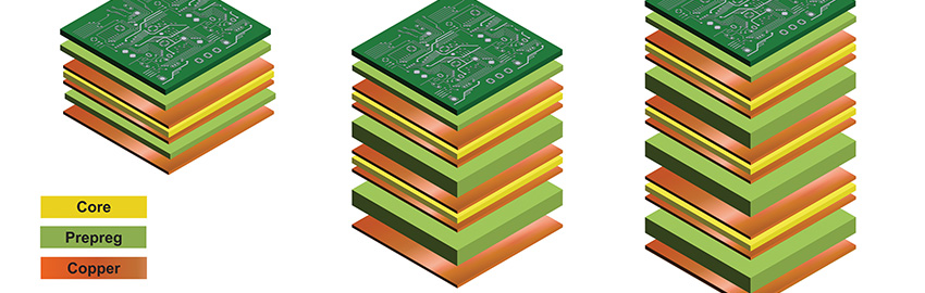
How the PCB Stackup Helps Control EMI
Power and signal placed on outer layers minimize radiated emissions.
READ MORE... -

Century Circuits
Which PCB technologies are best suited to survive 100 years?
READ MORE... -

Learning from the Past
What history can tell us about our position in high-tech.
READ MORE... -

Thermal Vias are Ineffective. Here’s Why.
Adding thermal vias can take up valuable board space with little benefit.
READ MORE... -

Connecting the Industry, from Boards to Assemblies
HDP is embarking on new rounds of evaluations of laminates and lead-free solders.
READ MORE...
Homepage Slideshow
How the PCB Stackup Helps Control EMI
Power and signal placed on outer layers minimize radiated emissions.
Century Circuits
Which PCB technologies are best suited to survive 100 years?
https://pcdandf.com/pcdesign/index.php/current-issue/241-designer-s-notebook/18061-century-circuits
Learning from the Past
What history can tell us about our position in high-tech.
https://pcdandf.com/pcdesign/index.php/current-issue/262-material-gains/18062-learning-from-the-past
Thermal Vias are Ineffective. Here’s Why.
Adding thermal vias can take up valuable board space with little benefit.
Connecting the Industry, from Boards to Assemblies
HDP is embarking on new rounds of evaluations of laminates and lead-free solders.


 As a career PCB designer, I’ve seen a lot of waves break over the electronics industry, but not since the very foundation of electronic computer aided design (ECAD) have I seen such a significant paradigm shift in our work practices. From the mid-20th century onward, computers have become involved with our design efforts. Aerospace and automotive industries led the way along with universities; about the only places where computers were available in those days.
