It was almost forty years ago when I got my first job as a freshman in Japan, and to celebrate my “success,” I bought a high-end watch made by Seiko –a large watch manufacturer in Japan.
When should machine soldering be used instead of manual?
High-mix production is the mainstay of many electronics assembly plants. Lot sizes and board complexities vary, and boards are often mixed technology, comprising a blend of both surface-mount and through-hole technology. Modularizing a production line enables a clear distinction between one type of assembly process and another. This month, we look at the decision-making of routing a circuit board through-hand assembly vs. automated selective soldering. This assumes a modern factory where a job can be routed to the selective soldering machine module, the hand assembly bench, or a combination.
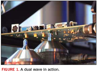
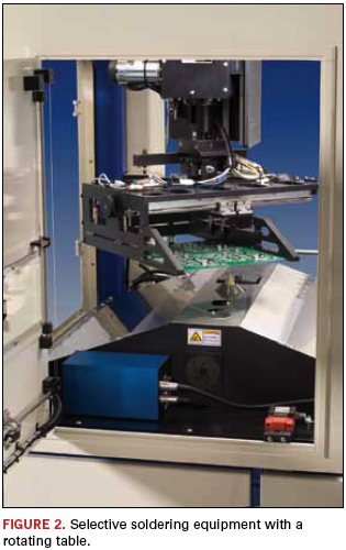
Selective soldering machines are an automated way to solder through-hole components on a circuit board. The machine contains a heated solder tank that generates a small fountain of molten solder approximately 0.375" in height and 0.25" in diameter. The leads to be soldered are positioned into this fountain of molten liquid for soldering (Figure 1) using a programmable x-y translation table. The operator places the PCB into the motorized x-y table (Figure 2) and by using a program (either input by the operator or imported from circuit board drawings), directs the board to move above the solder jet, lower a specific component into the solder fountain for soldering, raise the board, and translate the board to the next component to be soldered.
Modularizing the production plant enables the manager to match the production rate and precision requirements of a specific job with the correct machine or machine operation. A clear example of this modular approach is a comparison between routing a job between a hand-soldering operation and a selective soldering machine. Some decisions are obvious. After programming and setup of a selective solder machine, the process operation will always yield the same quality solder joint, repeatably. Hand soldering results can vary depending on the operator. This variation can be minimized if the assemblers are all trained to an industry standard like J-STD-001, Requirements for Soldered Electrical and Electronic Assemblies. This standard must be applied to the finished assembly, regardless of method of assembly, manual or automated.
Although surface mount is the dominant form of component today, some components may only be available in a through-hole format (such as power transistors and connectors). When a modular production line is set up, the decision of routing the job through the selective soldering machine may be based on the number of solder joints. If there are dozens to hundreds of joints to be soldered, the selective soldering path is a superior choice over a manual bench operation. If there are only a few joints to be soldered, hand assembly is a good choice.
Whether using manual or selective soldering, the board must be inspected by a human operator. This can reduce the efficiency of the automated process. With this in mind, the best modular location for the selective soldering machine might be in the hand-assembly department, where the employees have the necessary experience to inspect the output of the selective soldering machine to industry standards.
ACI Technologies Inc. (aciusa.org) is the National Center of Excellence in Electronics Manufacturing, specializing in manufacturing services, IPC standards and manufacturing training, failure analysis and other analytical services.
Several noncontact methods exist, but are they practical?
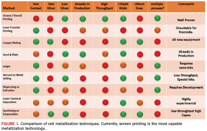
As a researcher and proponent of screen-printing technology (and, of course, an employee of one of the world’s top mass-imaging organizations), you may find it strange that I’m writing about alternative solar cell metallization technologies. But these other approaches do exist, and it’s important to understand them – and why many experts with no vested interest in screen printing still view the latter as the most viable, at least for the medium-term future.
Many alternative techniques have been around for a few years, and concurrent with their development has been the claim that one or more would displace screen printing as the reigning technology. So far that hasn’t happened, for two reasons: 1) Printer and paste manufacturers have kept pace with the latest demands for fine-line printing (we’re now sitting at 60µm wide lines in production and well below 50µm in a lab environment); and 2) the requirement for much thinner silicon (which would be subject to potential damage by the contact of printing’s squeegee pressure) to reduce cost has diminished in recent years, as the price of silicon has gone down by more than half.
Generally, the alternative metallization methods described below were applied to solar to reduce costs or to increase efficiency. In some cases, this was largely driven by the need to deposit material in a noncontact process to enable thinner silicon use. Each has its perceived advantages compared to screen printing (primarily noncontact techniques), as well as its drawbacks.
Laser transfer printing. This is a noncontact technology that uses a continuous tape loop and doctor blade arrangement to deposit paste, then locally heat the paste with a laser, which ejects the paste from the tape onto the wafer. Although nothing touches the wafer and the consumables costs are relatively low, this method cannot currently produce fine lines in high-volume manufacturing, and, consequently, the only viable market for it is for printing the back side of solar cells. Throughput is also fairly low.
Electroplating. This process – used also in semiconductor and printed circuit board fabrication – employs a chemical method to remove the silicon nitride locally, plate with a material (likely electroless nickel) to make the first contact with the wafer and electroplate the bulk copper on top of that. Because of copper’s corrosion problem, it then has to be passivated with a tin layer. The advantages of electroplating are the ability to produce ultra-fine lines with high conductivity and eliminate costly silver pastes. However, it does require three wet chemical processes that are time-consuming, labor-intensive, messy and waste-producing. This method also requires fairly high skills.
Seed print and light-induced plating. Either a screen- or an inkjet-printed low aspect ratio line is deposited with standard silver paste, and then silver is electroplated using the current generated by the cell itself during light exposure. In my view, the benefits of this technique are quite limited; there is a bit of extra conductivity from the silver because the electroplated silver is solid (as opposed to the honeycomb effect of fired silver paste), and there is reduced shadowing from the ability to plate narrow lines. But, the lines are limited to 50/60µm widths, which can be achieved already with screen printing. The disadvantages of a two-stage process, the additional capital expenditure for plating equipment, the line width limitations, and the chemical waste outweigh the marginal benefits.
Inkjet printing. This technology has been around for a long time and has various commercial applications. Initially, advocates thought it would be ideal for noncontact solar cell printing because of the historic success with inkjetting materials. But, inkjet printing requires low viscosity materials with nano-particles, so the paste is more expensive than traditional silver paste. Plus, most inkjet systems are challenged by high aspect ratio printing and need 10 to 20 passes to get the required height. The multiple passes obviously lower throughput significantly. There are also nozzle blockage issues. All in all, I think it’s very impractical for solar cell processing.
Aerosol or metal jetting. With aerosol or metal jetting, material is guided by pressurized gas and deposited onto the substrate. This method is noncontact, can do ultra-fine lines and has the positional accuracy of deposition. However, like inkjet printing, it is plagued by its inability to deliver high aspect ratios at high speed and also requires special inks.
Dispensing or extrusion. Automatic dispensing (also referred to as extrusion in some cases) for solar cell metallization is not that different from what is commonly used in electronics assembly. This is a needle dispensing technique where pastes are transferred in a non-contact method from the nozzle to the substrate. Dispensing is capable of achieving high aspect ratio line widths of 50µm, with further reductions likely, and has good positional accuracy. The drawbacks include the required use of special (read: expensive) pastes, nozzle blockage and low throughput.
Laser chemical metal deposition. Largely an experimental technique, laser chemical metal deposition is likely a few years away from any sort of commercialization. With this process, the solar cell is immersed in an electrolyte; a laser shines through the electrolyte, ablates an anti-reflective coating and causes activity in the emitter layer, which electroplates nickel lines. The advantages are its noncontact capability and the elimination of silver. If and when it becomes commercially viable, these advantages will have to be weighed against the associated waste, health and safety issues of a wet process.
Sputtering or evaporation. These technologies have been used in the semiconductor industry for a long time. Because they are semiconductor-accurate, extraordinarily fine lines and high aspect ratios can be achieved in a noncontact process. What’s more, just about any metal or stack of metals can be deposited. On the downside, sputtering and evaporation are very slow and require a high vacuum process. Throughput is adversely impacted by the requirement to have everything go through a vacuum chamber first. There are also tooling costs associated with making the photolithography resists used to define the plated or metal-coated areas. If this is achieved through a mask, then that is a tooling cost as well. Currently, the capital expenditure costs are high, but there is industry chatter about these techniques becoming more useful for backside aluminum.
So, there you have it: the pros and cons of screen printing alternatives to solar cell metallization. Currently, there is no other method that can deliver the aspect ratio or speed efficiency of screen printing. The technology’s inability to offer noncontact material deposition seems to be a moot point, if and until silicon wafer thickness begins to diminish. Even then, modern printing systems can effectively manage wafers as thin as 120µm with very low breakage rates. And while printing can’t eliminate silver pastes until there are fully functional, commercially available non-silver pastes, it can assist with reductions in silver consumption right now. Using print-on-print (POP) and dual print technologies, the cost impact of silver can be significantly mitigated. (“Strategies to Offset the Rising Cost of Silver,” "CIRCUITS ASSEMBLY, September 2011.) For the time being, I am of the firm opinion that screen printing is the most cost-effective, efficient method available for solar cell metallization.
[Ed.: To enlarge the table, right-click on it, then click View Image, then left-click on the table.)
Hurricane Sandy poured rain on most contingency plan parades.
A funny thing happened on the way to – in fact just before – the recent US Presidential election. A mysterious lady showed up on the scene. Not necessarily a pretty one, but one bearing a larger than life persona who successfully took the mind of everyone within her wide swath off the election, or for that matter, everything else. That mysterious lady’s name was Sandy, and she again reminded those on the Atlantic Coast the US of what is really important.
And while those in other parts of the globe missed Sandy’s wrath, anyone who experienced the earthquake in Japan during 2011, the tsunami in Thailand that fall, or any of the typhoons that frequent the Southern Hemisphere understands the feeling of going to sleep one night with one plan only to wake up the next morning to a new world in which all notions of what’s important are turned upside down.
So what is important? Everyone would agree family and friends, health and safety. I would argue that relationships between customers and suppliers are important too. Possibly most important is the commitment to making sure that those within your scope of influence are protected from the misfortune and risk that natural and not-so-natural phenomena could cause.
Disasters have an uncanny ability to refocus us on the importance of contingency planning. Contingency planning is similar to other forms of “strategic” or “tactical” planning, except instead of considering desirable “what if” scenarios, it requires expending thought and effort on darker outcomes. Those dark outcomes include natural events (in insurance parlance, “acts of God”) such as fires, major storms, earthquakes, flooding, etc. But the dark side of “what if” also should include the consciously made “self-inflicted” decisions that sometimes just do not work out as planned and take a decidedly disastrous turn.
The easier, albeit not necessarily easy, contingency plans are those related to natural disasters. We all fear – and understand – the “what if” of a flood, storm or fire ravaging our facilities or their immediate surroundings, yet regrettably too few of us have an adequate contingency plan detailing how we would respond. For years, when asked what I would do if my plant burned down, I have jokingly replied, “File for Chapter 7.” But a simplistic approach is simply not the answer! There is so much more to consider: employees, customers, suppliers. The reality is that whether a major, game-ending event, or a minor one, a real plan needs to be thought through and ready for that “what if.” For those who do have a plan, should something happen to their individual facility, what if a disaster impacts more than just your site? What if a storm such as Sandy impacts a large region, or earthquake or tsunami devastates an entire country? How will your Plan B hold up in the case of such an event?
More difficult to plan for are those events caused by self-inflicted, poorly devised or executed decisions. Some could argue that a decision that could be as disastrous as even the worst storm is when management’s decisions exaggerate the natural workplace stress to the point of employee unrest or even suicides. Whether responding to a natural disaster or a manmade one, the outcome will be far worse without adequate contingency planning.
How do you plan for the unthinkable? Start by making a list of the stakeholders. Knowing who must be protected is a great first step toward planning protective actions. Safety and health come first, so the immediate catastrophe response most companies already have in place should be the foundation of any plan. Next is mapping a game plan that will assure customers and suppliers have a clear direction as to what you plan on doing, where and when. This planning is just as important as the safety of employees, as without customers and suppliers you might never reemerge from a disaster.
Next in the decision tree should be to map a plan for things you cannot control – external issues such as infrastructure destroyed to the point that even if your facility and employees come through unscathed, the ability to function is rendered impossible. This type of planning can only be done by conferring with local authorities so you understand their plans in the event of such a disaster. While never perfect, if minimally you end up at least knowing who to talk with in a given situation so you can determine the appropriate course of action in the case of an emergency, you will be far better off.
None of this is rocket science. The problem is, as simple as it may be, few of us actually have undertaken the effort to think through, communicate and document a contingency plan with the appropriate input from internal and local stakeholders.
And as few who have done any contingency planning for natural disasters, even fewer have thought through what to do if their decisions cause a life-threatening environment and/or disaster. Yes, individual conscience must dictate what types of events would be considered such a disaster; however, we should think through the typical decisions a company dealing with people, chemicals, equipment and deadlines makes and what to do if the outcome of those combined decisions has potentially life-threatening consequences.
So, while cruising along focused on an election, fate struck with a terrible storm and quickly refocused so many. We need to stay focused on making sure that when fate strikes, be it natural or self-inflicted, we have a well-thought-out contingency plan to help us through.
A look back at friends and colleagues who left us in 2012.
A pair of true industry giants died in this past year, both pioneers in their own right. Olin King founded Space Craft Inc., which under its more common name SCI Systems (and later, Sanmina-SCI), is generally recognized as the first contract electronics assembler and, for a time, was also the largest EMS company in the world. For his part, Gene Marsh was an electronics design automation pioneer, bolting Raytheon for a career developing PCB software for the masses. The Gene Marsh Award for Technical Innovation is named for him.
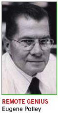
Two other major league inventors also passed this year. All couch potatoes owe a nap of gratitude to Eugene Polley, who over his 47 years at Zenith rose from stock boy to become assistant division chief of Mechanical Engineering and counted the first wireless remote control among his 18 US patents. And anyone who sees the promise of green energy can appreciate Stanford Ovshinsky, who was assigned more than 400 patents, the most significant of which – the NiMH battery – is used in everything from laptop PCs to cellphones to electric cars, and who later developed flat screen LCDs and thin-film solar cells. This month we reflect on their impact on our industry and our lives.
(Harold) Gene Marsh, 84, launched PADS Software in 1975, one of four companies he founded.
Olin King, 78, founder Space Craft Inc. (later, SCI Systems); credited with founding the modern contract electronics assembly industry.
Robert (Bob) Bukowsky, 71, former IDEAL vice president of sales.
James Lee, 51, founder of PCB fabricator UniGlobal.
Mr. Xie, age unkown, Foxconn employee.
Steve Appleton, 51, CEO of Micron Technologies.
Jackki Morris-Joyner, longtime IMAPS technical program manager.
Stanford R. Ovshinsky, 89, semiconductor expert who invented the nickel-metal hydride battery and codeveloped solar energy panels and flat-panel displays.
Robert (Bob) Parker, 53, computer engineer at Universal Time Co.
David B. Speer, 61, ITW chairman and CEO.
Chris Lewis, 64, president, CEO, and co-founder of Dynawave Inc.
Hans Camenzind, 78, analog guru who introduced the phase-locked loop to IC design.
Mr. Yang, 22, Foxconn Shenzhen.
Eugene Polley, 96, longtime Zenith Electronics engineer and inventor of the wireless television remote control.
And one in late December 2011:
Gene Hendrickson, 79, former Tektronix engineer, president of General Management Integration (GMI), and founder of the October Project.
It was a fairly quiet year for acquisitions. AsteelFlash, a former CIRCUITS ASSEMBLY EMS Company of the Year, and Creation Technologies, this year’s winner (see story, pg. 30) made their near-obligatory deals, but for the most part, the top two EMS tiers were quiet, while Viasystems’ purchase of DDi and Cadence’s acquisition of Sigrity, respectively, were the largest two fab and design deals. Then in early November, the earth was shaken by two huge announcements.
In early November, just days after Cookson announced it would split in two and spin out Alpha Metals and Enthone as a separate company, Dover said it too would divest its electronics assembly and test businesses. And just like that, we are primed to lose two of the longstanding electronics supply-chain brand owners.
For Cookson customers, the first question must be, what will this mean for Alpha and Enthone? My take is not much. Here’s why:
1. The company will remain public, and the shareholders are the same. (Under the proposal, Cookson shareholders get one share in each of the two new companies.) Had this been an MBO or private equity deal, I would expect slash and burn. But the transition as planned should bring much-desired stability to the new organization.
2. The upper management isn’t changing. Had Cookson Performance Materials group CEO Steve Corbett left, I might think differently. But Corbett, who joined Cookson in 1990 and has run Enthone since 2002 and both companies since 2004, is highly responsible for the existing management and operational structure. He knows what he is doing, knows the markets and understands the brands.
3. The debt is manageable. Alent (the new name of the former Cookson Performance Materials) will “get” about one-third of Cookson’s £451 million ($727 million) worth of debt. Given the new company’s sales of £418 million ($675 million) and profitability, it should be able to swallow that meatball.
4. The brands are intact. The Alpha and Enthone brands are well-recognized and respected worldwide. Indeed, after spending some time trying to beef up the somewhat unwieldy Cookson Performance Materials name, the company reversed gears and has been working over the past year to rebuild those individual brand names. Perhaps this was in anticipation of the demerger, but either way, the strategy was well-timed.
In fact, the only casualty I see in all this is the 300-year-old Cookson name. One wonders whether it was seen as a negative by either of the spinoff companies. And so goes Cookson. From its founding by Isaac Cookson in 1704 as a collection of metal and glass businesses to its aggregation and subsequent divestment of a herd of electronics equipment and materials companies in the 1980s and 1990s, Cookson has always been in a transition of some sort. This latest move appears to be its final one.
As we went to press, the future of the Dover businesses was much less clear. Dover hasn’t said whether it will sell the businesses piecemeal, as it did with Universal Instruments and Vitronics-Soltec in 2006. The brands on the block – DEK, OK International and Everett Charles Technologies among them – probably brought in at least $1 billion in annual revenue prior to 2012’s drop-off, and have traditionally been higher margin performers as well. Not many equipment companies have pockets deep enough to absorb the price Dover will ask. Yet that’s what employees of those businesses must be hoping for right now, as the scorched earth tactics of the private equity companies have been excruciating for everyone involved.
We don’t think this was a quick decision brought about by this year’s slump. Sources tell us Dover has been discussing the possible divestiture of these businesses for nearly a year. The guess here is that Dover’s management is tired of the endless boom-bust cycles of the electronics industry. It’s hard for an equipment company to meet Dover’s goal of 10% revenue growth and 15% operating margins year in, year out. We also believe Dover has a buyer on the hook, as some might recall that when Dover announced the impending divestiture of Universal, the deal went through a month later. Who that buyer is (ITW? Nordson?), and at what price, are now the questions.
Urgent ‘bulletin.’ In November, we launched Board Talk, the bulletin board for the PCB industry. The new board – theprintedcircuitboard.com – has categories for PCB design, fabrication, assembly, market data, trade shows and press releases. Members are invited to create their own topics (threads) for discussing anything industry related that they have on their mind.
We also are happy to announce an agreement with the IPC Designers Council to offer Board Talk as a communications center for news, announcements and meetings, plus information on the Designers Certification program. Please check it out.