Simple constraint and design rule checks can set the maximum stub length.
It’s no secret that placing passive devices in the proper location, whether nearer to the source/driver or the receiver/load pins, is the difference between poor signal integrity and optimal signal integrity. Often this can be impacted by a breakdown in communications between circuit designers and PCB designers.
Typically, the circuit designer has the background information such as distance and constraints, and can determine best the placement of these devices. However, this information may not be provided to the PCB designer during the initial placement phase, leaving them in the dark.
The following are tips on how to achieve the correct placement of passive devices, including a look at the maximum stub lengths option that helps avoid improper placement issues.
Tips for proper placement of passive devices.
1) Perform a manual check of vendor specifications for component placement and topologies.
- The circuit designer should share the vendor specifications of the devices with the PCB designer.
- The PCB designer carries out the checks per the specifications that apply to physical layout.
2) Work with the circuit designer to gain a comprehensive understanding of the vendor specifications by asking questions like:
- Are there length- or delay-based requirements to control skew?
- Are there critical placement requirements for termination devices?
- Are there required routing topologies that must be followed to maintain proper stub lengths, i.e., applying daisy chain or star topologies?
3) When the design is complete, work together on the circuit simulation to understand where errors may be and put together a comprehensive design rework plan to eliminate further cycles of simulation and rework.
There is another way to tackle this problem that eliminates some issues related to critical placement of termination devices. You can use a simple constraint and design rule check. The circuit designer can set constraints that the PCB designer can then apply to the design using CAD software. The rule known as “maximum stub length” can be further controlled using a graphical topology editor.
What is maximum stub length? When I instruct PCB designers in high-speed constraint management and routing classes, I always ask this question: “What is maximum stub length?”
The most common answer is: “It relates to the routed trace stub from an SMD pin to a via.”
Depending on the PCB design software being used, the answer is not completely wrong. In all honesty, I don’t expect PCB designers to know the answer. In fact, many PCB designers agree that it is the circuit designer’s job to know this and to communicate the rules to them.
Maximum stub length is the length at which the trace will start to behave as a transmission line and at which it becomes capable of causing signal reflections. This behavior occurs when routed signals are branched off using what PCB designers refer to as tee-routing, or routed lengths to termination devices are too long.
The premise is that physical length must match a timing requirement set according to the manufacturer’s measured results of the ICs on a test fixture.
Many other forces and factors are at work here, but the point remains the same: when routing a daisy chain topology, PCB designers try very hard to avoid tee-routing patterns. While this is a good rule of thumb, there may be a little more leeway than one would expect when observing maximum stub length values.
Using the maximum stub length constraint. While it’s not the PCB designer’s role to challenge the manufacturer’s specification, it is ordinarily the circuit designer’s responsibility to provide this information in the form of a constraint or rule (not just as text notes). This small added step provides big benefits with an additional design rule check to seek out violations of the maximum stub length rule, and at the same time, it can also be used to help with the placement of passive devices used for termination.
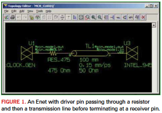
The simple topology in Figure 1 shows an Enet with the driver pin passing through a resistor and then a transmission line before terminating at a receiver pin. Using a constraint browser and topology editor for schematic capture in combination with signal integrity simulation, circuit designers can graphically create and simulate the effects of stub length using pin symbols, components and transmission lines. No more handwritten notes, hand routing, clock signals, etc.
When the circuit designer provides the stub length values, the PCB designer has rules to guide the placement of the devices. The PCB designer places devices on the PCB layout and sees a dynamic fence appear along with constraint indicators as guides (Figure 2).

By constraining stub lengths through passive component placement using CAD software, designers can overcome challenges associated with the improper placement of passive devices used for Enet signal termination.
Andy Buja is a senior applications engineer for CADStar and CR-5000 at Zuken; This email address is being protected from spambots. You need JavaScript enabled to view it..


