Typhoon Haiyan swept through the Philippines leaving a trail of damage and destruction. The typhoon was the strongest typhoon to make landfall in recorded history. It is estimated that more than 10,000 people are dead or missing, and millions more remain homeless.
“Fine Pitch Reliability Comparisons between Components Assembled on Motherboards with Filled and Unfilled Microvia-in-Pad”
Author: Denis Barbini, Ph.D.; This email address is being protected from spambots. You need JavaScript enabled to view it.. Abstract: Fine-pitch surface-mount WLCSP and CSP devices often require printed circuit boards containing microvia-in-pad for complete route-out. Often the microvias are left open, or “unfilled.” The resulting solder voiding and routing design can presumably alter the reliability of the assembly when compared to a plated shut, or “filled” via. This study was designed to compare the reliability of fine-pitch (i.e., 0.5mm and below) components assembled on filled and unfilled microvia-in-pads using thermal cycling and drop testing. (SMTA International, October 2013)
Component Packaging
“Trends and Considerations in Automotive Electronic Packaging”
Authors: Deborah Patterson, Marc Mangrum, Adrian Arcedera and John Sniegowski; This email address is being protected from spambots. You need JavaScript enabled to view it.. Abstract: Semiconductor growth is accelerating with a rapid transition from mechanical to electronic systems. An important part of winning automotive business is in having package platforms that pass demanding automotive requirements. Automotive manufacturers strive for a “zero defect” policy on all components found in a car. A package may look like a standard product, but it may actually utilize special materials, processes or construction. Includes a list of the discussion points that make automotive packaging different. (Meptec Report, vol. 17, no. 3, Fall 2013)
Component Reliability
“Additive Manufacturing Technologies for a Direct Integration of Microelectronic Components and Contact Structures” Authors: David Ifland, Frank Ansorge, Christian Baar and Klaus-Dieter Lang. Abstract: System-in-package (SiP) modules were manufactured using an additive manufacturing process. In this case, electrical components are integrated in the manufacturing process of the support substrate. An electrically conductive adhesive was then applied. This feasibility study demonstrates a novel three-dimensional construction and connection technology for microsystems. (Leuze Verlag, August 2013; http://leuze-verlag.de/en/fachzeitschriften/galvanotechnik/aktuelles-heft/mikrosystemtechnik)
“Process and Material Envelope for Allowable Package-on-Package Warpage” Authors: Pradeep Lall, Ph.D., Kewal Patel and Vikalp Narayan; This email address is being protected from spambots. You need JavaScript enabled to view it.. Abstract: Package-on-package (PoP) assemblies may experience warpage during package fabrication and later during surface mount assembly. Excessive warpage may result in loss-of-coplanarity, open connections, misshaped joints, and reduction in package board-level reliability (BLR) under environmental stresses of thermal cycling, shock and vibration. Previous researchers have shown that warpage may be influenced by a number of design and process factors, including underfill properties, mold properties, package geometry, package architecture, board configuration, underfill and mold dispense and cure parameters, and package location in the molding panel. A comprehensive inverse model incorporating a full set of design and process parameters and their effect on PoP package and PoP assembly warpage is presently beyond the state of art. In this paper, data have been gathered on multiple package-on-package assemblies under a variety of assembly parameters. The packages have been speckle-coated. The warpage of the PoP assemblies has been measured using a glass-top reflow oven using multiple cameras. Warpage measurements have been taken at various temperatures of the reflow profile between room temperature and the peak reflow temperature. Finite element models have been created, and the package-on-package warpage predictions have been correlated with the experimental data. The experimental data-set has been augmented with the simulation data to evaluate configurations and parameter-variations that were not available in the experimental dataset. Statistical models have been developed to capture the effect of single and multiple parameter variations using principal components regression and ridge regression. Best subset variables obtained from stepwise methods have been used for model development. The developed models have been validated with experimental data using a single factor design of experiment study and are found to accurately capture material and geometry effects on part warpage. The results show that the proposed approach has the potential of predicting both single and coupled factor effects on warpage. (SMTA International, October 2013)
This column provides abstracts from recent industry conferences and company white papers. Our goal is to provide an added opportunity for readers to keep abreast of technology and business trends.
My latest copy of National Geographic contains an intriguing article about the value of failures in exploration, such as Ernest Shackleton’s famous expedition in the Antarctic, and how the experiences (though sometimes tragic) paved the way for future success.1 After providing numerous examples of failures, the article discusses lessons learned that enabled progress in future explorations, or some realized benefit greater even than the original goal. Failure the first time is an option, the article explained, and many Silicon Valley companies experience disappointing results before ultimately finding success in alternative products or in future companies the founders go on to establish.
One relevant and more current example is Apple’s Newton device, a failure that provided valuable insights toward a future success: the iPad. While few remember the Newton, which debuted in 1993, everyone knows the iPad. It makes one consider some of today’s products and the insights they might provide for technologies of the future.
What about some of today’s products? Will there be a success or a failure that leads us to some greater innovation? Casio introduced a camera watch many years ago that enabled the user to record video (in black and white). It was fun to play with, but I would not consider it a huge commercial success. Today Samsung, Sony and others have new smart watches with improved features. Another consumer product coming to market (with a fairly high price point – around $1,500) is Google Glass. The success or failure of this product remains to be seen. Interviews with several users offer insight into its application, however. A software programmer who is also a Glass Explorer (the group of developers that signed up to get Glass during Google I/O 2012) uses his glasses to monitor the many emails he receives to determine which require action. A recent Carnegie Mellon University graduate discusses how the glasses can be used by medical students to watch a surgery or by an anesthesiologist to monitor a patient’s vital signs while administering anesthesia. Hollywood stars were provided with Google Glasses at a recent red carpet event. Some of the press also had Google Glasses to interview the stars, and the hands-free video capability was entertaining. These may be niche applications, and the product may be too geeky to hit as big as the smartphone or iPad, but it also may provide valuable information that can help develop the next generation of wearable electronics.
Wearing the future. Wearable electronics include a multitude of potential consumer products, not just virtual reality eyeglasses and smart watches, but sophisticated health monitoring devices using elastic wristband or headbands, canes with sensors for the blind, and other clever products. Wearable electronics for soldiers on the battlefield will likely become a near-term reality.
InteraXon, a Toronto-based startup, has introduced Muse, a headset with the form of a comfortable headband that contains six sensors that monitor brain activity. The product, which sells for $269, is said to enable users to understand how their brains work, and to attain peak performance, reduce stress and enjoy better brain-related health.2
Plenty of work remains before wearable electronics become reality for many consumer applications. Improved battery technology with recharging capability will be critical. A recent Intel Developer Forum discussed ultra mobile devices and requirements for low-power processors such as the Intel Quark processor family. Expect additional announcements of low-power devices. Ultra thin chips, perhaps embedded in flex-circuit or thin laminate substrates, may also enable a key future product. Wafer-level packages enable Casio’s first camera watch and will likely do the same for any future wearable electronics.
Whether today’s products are a big hit does not matter. Total commercial success is not required, and failure is OK. What is important is that the developments of today will pave the way for some exciting future consumer products.
A final thought: Although some of today’s products may not be a total commercial success in terms of sales, they will provide the learning experience that enables future generations’ killer apps.
References 1. H. Bloch, “Failure Is an Option: Where Would We Be Without It?” National Geographic, September 2013. 2. P. Moreira, “When the Muse Headband is Upon You, It Senses Brainwaves,” USA Today, Sept. 26, 2013.
The new PCB flatness guidelines cover machine selection, measuring and testing, to which our author adds some best practices.
IPC-9641, High Temperature Printed Board Flatness Guideline, has been approved and released by IPC. For the first time, an international standards organization addresses local area PCB warpage across reflow profile temperatures. The standard provides guidelines for selecting measurement equipment, planning testing, preparing PCBs for test, performing measurements across reflow temperatures, and reporting local area warpage results.
Measuring and controlling package warpage across the full thermal reflow profile has been standard practice for years and is seen as critically important to final product yield. IPC-9641 has been approved because IPC members have determined that, as stated in the introduction to the standard, “… controlling the board flatness is equally important for preventing subsequent assembly-related issues, including open or bridging joints, which ultimately cause product failure.” Assembly-related issues also include challenging problems such as head-in-pillow that ultimately lead to field failures and product returns. So, while for many years the package was held up for scrutiny as the only relevant contributor to warpage-related assembly defects, now the other side of the attach interface, the PCB land area, has also been identified as a potential contributor to defective assemblies. It’s now important to understand, quantify and control the warpage of PCB areas where packages attach across temperatures.
The standard is both educational about the general topic of PCB warpage measurement and specific in its guidelines for how such measurement should be done. The standard provides a starting point and a point of reference as companies begin to build, or to improve, PCB warpage measurement systems. As an additional benefit, when dynamic warpage information is obtained from PCB areas, these data can be shared with those responsible for package manufacturing and SMT assembly to facilitate continuous improvement in both component shape compatibility and final product quality.
The rest of this article consists of a summary of the contents of IPC-9641, followed by some notes about how to implement it using practical best practices derived from years of measuring packages and PCBs.
Section 1 – Purpose. A concise statement of the purpose of IPC-9641 comes from its introduction: “This document aims to provide guidance on methods and procedures for critically evaluating printed board flatness during a simulated temperature reflow cycle.”
This section introduces the intent of the standard, explains its scope and how it differs from existing standards, and includes a glossary of terms that are defined to provide a common understanding of meanings of the warpage-related technical terminology that appears later in the document. It also lists other documents and standards (such as Jedec JESD22-B112) that preceded this one and can provide appropriate historical context. For those involved with warpage measurement, the glossary may serve as a useful reminder, and for those not yet measuring warpage of any type, it may serve as an invaluable reference.
Section 2 – Applicable documents. This section is simply a list of all related Jedec, IPC, and Joint Industry Standards, for serious students of the subject who want to review all available publications from these bodies that provide context for IPC-9641.
JESD22-B112, High Temperature Package Warpage Measurement Methodology, is the most closely related standard on the list. It details a method for consistently measuring package warpage, like IPC-9641 addresses measuring the corresponding land areas on PCBs.
Section 3 – Measurement instrument requirements. This section reviews different metrology technologies and the theory behind how they work. It is the most purely “educational” section of the document, and explains shadow moiré, projection moiré, fringe projection, confocal and optical coordinate measurement technologies. These are the metrology methods for PCB local area warpage measurement “recommended” in the standard. (Each technology is only briefly discussed, and pros and cons or tradeoffs for each technology are not fully addressed, so this section is best used as an introduction to the topic of potential measurement technologies, and supplemental research would be prudent.)
Section 4 – Parameters of interest. This section lists contributors to PCB warpage, including design and manufacturing variables. It notes that it is easier to change the manufacturing parameters than the board design itself.
The effects of clamping and board support methods are explored. Diagrams and static equations illustrate the mechanical effects of constraining the PCB during reflow assembly. The purpose of this section is to emphasize the importance of mechanical support and clamping constraints as variables to be considered and dealt with appropriately when making decisions about warpage measurement methodology.
Section 5 – Recommended test methodology. This section includes recommendations for how to control variables that exist when making thermal warpage measurements on PCBs. Subsections include:
Preconditioning/preparation of samples – replicate as close to production preparation as possible.
Number of samples – for valid results, use the listed minimum number of PCBs per test.
Thermocouple placement – attach following recommended placement and method.
Specific temperatures for data acquisition and ramp rates – measure at temperatures across the reflow cycle, with ramp rates as high as possible with an acceptable temperature gradient.
Recommended test methodology – includes an example reflow profile with measurement points shown.
Data reporting – provides example of third graphs with signed coplanarity gauges as results.
Section 6 – Metrology accuracy for printed board flatness. This section provides an example of how to verify that measurement equipment performs accurately across all relevant temperatures. The process involves measuring the surface of a material that does not noticeably change shape as temperature changes (due to a low coefficient of thermal expansion) at multiple temperatures across the reflow profile. The gist of this section is that there are ways to “prove” that results from a piece of equipment are valid at all measurement temperatures.
Implementing IPC-9641
Due to customer request, assembly problems, quality assurance needs or some other driver, companies may need to start implementing the standard and begin measuring land areas on PCBs for warpage across the reflow profile.
The general information and best practice suggestions that follow apply to all the measurement technologies recommended in the standard. To be clear, these are recommendations from the authors that have been developed from years of measuring warpage in various customer applications, but are not included in the text of IPC-9641.
Equipment selection. Those who have been measuring warpage at elevated temperatures are halfway to implementing the new standard. It’s likely that companies want to use the warpage measurement system they have on hand. For those who don’t have equipment to access, choosing the measurement, analysis and reporting system to be used will be an important decision. Some things to keep in mind when evaluating options:
Desired z-resolution. Z-resolution is how closely the equipment can “trace” the actual surface to deliver accurate data. It’s usually defined in microns. For example, a system with 5µm z-resolution would be able to distinguish between two points on a surface that had heights that were different by 7µm, but a 3µm height difference would likely not be measured. (The height difference would be reported as flat.) Package designers and manufacturers typically desire a z-resolution in the 1 to 3µm range. For PCB areas, 5µm or less is recommended.
(For fringe-based systems, z-resolution is a function of fringe density. For confocal and other optical point-based systems, z-resolution is a function of the speed setting, optics and light source used.)
Desired data density (XY). Confocal methods will provide slow point-by-point measurements, making the XY density of necessity low. While other optical methods can measure hundreds of thousands of points in 1 to 5 sec., confocal is a scanning technique that can only deliver a few points in that amount of time. So the tradeoff for extremely precise z-resolution is very poor XY resolution.
Expected volume of measurement. How many measurements will be required per day and the throughput capability of the system(s) being considered should be estimated. Typically, fringe projection and shadow moiré provide the fastest speeds, while confocal and OCM systems take longer, as noted in the standard.
Planned correlation with suppliers and customers. The decision of which technology and specific equipment to use can become complicated, or sometimes simplified, when the capabilities and plans of supply-chain partners are considered. If there is intent to share data among multiple parties, it would be appropriate to make a group decision about what measurement technique will be used and what data correlation format will be shared.
Accuracy at high temperatures. Once the measurement system has been acquired and learned, IPC-9641 recommends verifying its accuracy across temperatures. The standard includes a guideline for how to establish accuracy capabilities. In doing so, users may want see results from the equipment vendor for its standard “accuracy across temperature validation,” and perform additional validation testing at the user’s facility on their equipment. IPC-9641 is a guideline. It intentionally does not attempt to detail system-specific methodologies. Equipment suppliers will likely have a more complete and detailed methodology that includes information such as proper sample surface preparation, safety protocols, etc., to use to establish equipment accuracy at elevated temperatures.
Preparing PCB samples for test. Once comfort with the measurement accuracy across temperatures that the measurement system delivers has been achieved, prepare samples for test.
IPC-9641 notes that, depending on moisture levels, PCBs may require a pre-bake process. From our experience over the past decade, and from testing many PCB designs during a PCB flatness study for iNEMI from 2009 to 2011, board moisture is a major contributor to warpage results, and a 12-hr. pre-bake should be seriously considered to remove moisture from boards to a consistent minimum level. This process will help control one of the variables that has a large effect on thermally-induced warpage. Alternately, if no pre-bake occurs before actual production reflow assembly, establishing the wider range of warpage and higher coplanarity results that represent assembly conditions may be a better approach. Across the package industry, pre-baking is the norm, especially since pre-baking and/or controlling package moisture levels with in-transit sealed shipping bags prior to assembly is common practice. Keep in mind that warpage levels will be much more in-control and consistent if the boards are prebaked before measurement.
Best practice: A 12 hr. pre-bake at 125°C is recommended for all PCBs.
Painting the surface. Most of the measurement technologies listed in IPC-9641 do not absolutely require sample surface preparation, e.g., painting them white. When using optical metrology, however, the best data possible (the data that best represent the actual physical surface being measured) result from the most ideal optical surface. And the ideal surface for optical measurement is diffuse and white. Unpainted surfaces yield results with more noise, and in some cases garbage results if the surface has too much specularity, such as with shiny copper traces or pads. Correlation will be much improved if all parties involved follow the same sample surface preparation method. The equipment supplier can recommend sample surface treatment steps to help get the best data.
Best practice: Painting the area of interest flat white is recommended.
Cutting the boards. To measure the package land area on the PCB, the PCB must fit into the oven of the measurement equipment. If a board is larger, trimming the board to fit is required. The rule of thumb is that the more material around the area of interest can be kept, the more “real” warpage results will be obtained. When cutting boards, induce as little mechanical and thermal stress as possible, such as by clipping them with shears. Best practice: Carefully trim the board to fit in the oven.
Attaching the thermocouples. The standard notes specific, preferred thermocouple attachment methods. A picture of the taping method, just off to the side of the painted land area-of-interest, is shown in Figure 1.
Best practice: Attach the driving thermocouple near, but outside, the package land area to be measured.
Fixturing the samples. The standard notes that there are various assembly fixturing techniques used in reflow assembly, including on-rails, simply supported (with at least one rail across middle), and different clamping methods.
Not fully covered in the standard is what to do about measuring the boards if they are normally clamped during assembly. This is especially relevant, since clamping the boards does affect warpage, and putting a board that is in a clamping fixture into the oven of the measurement equipment will likely not work, if the fixture blocks heat transfer to the board. Many, but not all, measurement systems use IR heating, and if the clamping fixture blocks radiated energy, it will not be possible to measure the PCB in situ with the same mechanical constraints in place as when it goes through the reflow oven. Measuring with a simple support setup and using that data to correlate with what the area will actually do when clamped is one alternate approach. However, the sample is supported in the oven – with two or three rails, on a flat glass sample support, a specialized fixture (Figure 2), or in its own clamping fixture. This setup should be established and communicated with all the supply chain partners in your correlation group.
Best practice: Fixture boards consistently for all measurements.
Establishing the thermal profile and measurement temperatures. Another method you should share with all your supply chain partners interested in board warpage is the thermal profile and measurement acquisition points you will use for each board design. Comparing results both between and within board designs, for different regions of interest, is facilitated by establishing a common set of temperatures that are important for decision-making. Measuring at multiple points is prudent, but it can become impractical to attempt to measure at every single degree, for example, since temperatures are changing quickly and each measurement takes some non-zero amount of time to complete.
Ramp rate, or the rate of change of temperature of the sample, is mentioned in the standard. The standard recommends setting the ramp rate as high as possible, provided it does not induce more than a 10˚C difference between the top and bottom of the sample. In our experience, a 0.5˚ to 1.0˚/sec. heating rate is ideal; though, with thicker boards that tend to impede temperature equalization, the target rate will need to be established with actual test results per board design. Best practice: A typical temperature profile with acquisition points is shown in Figure 3.
Taking measurements. After all this preparation, it’s finally time to take some measurements. The board is in the oven; the profile is set; the automated acquisition software is run, and the machine does the rest. An example of raw data from a PCB land area, measured with shadow moiré technology, is shown in Figure 4.
Best practice: Run the thermal profile, and obtain measurement data only at important temperature points.
Analyzing and reporting the data. Analyzing the raw data results by following a common method is required if data are to be correlated with other parties. The amount of data smoothing, data density and other variables need to be controlled as closely as possible to get the closest resultant correlation. Preparing results in a table or 3D visual reporting format are common ways that package suppliers communicate dynamic warpage. With enough samples measured throughout a temperature range, and associated analyses run, this complete process is sometimes called the warpage characterization of components such as packages and PCBs.
Best practice: Process data according to a common methodology shared among supply chain partners. Create template-based reports to share.
Number of samples. Establishing a statistically acceptable set of results will depend in part on how many samples are tested, of a given lot of a particular design. The standard recommends testing a minimum number of PCBs to establish the performance characteristics of the lot; although, testing more may give a higher confidence level that a representative range and standard deviation have been properly established. Generally, the warpage tendency of a particular PCB lot is usually clear once 10 samples have been measured.
Best practice: Test enough boards per lot to effectively “characterize” the lot’s expected warpage across temperatures.
In releasing IPC-9641, High Temperature Printed Board Flatness Guideline, IPC has indicated that making assumptions about the warpage of one side of that interface – the package land area on the PCB – is no longer sufficient for the design of reflowed assemblies. We are moving toward an era when the shapes of the components attaching during reflow will be compared and constrained at each temperature, and the compatibility of those shapes will tell us what needs to be done to get the best product yield, as well as what final quality level can be expected from their combination. Measuring the reflow-induced warpage of package land areas on PCBs is a big step in that direction.
Acknowledgments
Information about thermal warpage measurement best practices in this article was provided and reviewed by the subject matter experts at Akrometrix, Ryan Curry and Neil Hubble. John Davignon not only led the subcommittee that developed IPC-9641, but also reviewed and contributed the foreword (online) to this article.
Existing advanced methodologies for cross-discipline co-design, and new methodologies for resolving their gaps.
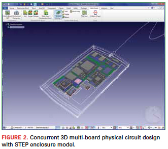
As products deliver more functionality, requiring greater electronic and mechanical design complexity, while also shrinking in size, packaging and electronics assemblies are becoming more tightly integrated than ever. Increasingly, packaging must take into account the physical properties of the electronics, while the electronics design is subject to even tighter mechanical constraints. Teams working on the electronic and mechanical aspects of the design need to continuously exchange design information to avoid wasting time on a direction incompatible with another discipline. Exchange of design information is currently limited, however, because the mechanical design is nearly always done in 3D, while the electronic design is done one board at a time in 2D or 2.5D. Neutral file formats such as Intermediate Data Format (IDF) pass printed circuit board data, yet the need to flatten the mechanical design before it can be used in an electrical computer-aided design (ECAD) system means that much of the design information is lost in translation.
New generation ECAD systems address this challenge by providing multi-board and native 3D design capabilities, along with direct translation to leading mechanical computer-aided design (MCAD) systems, enabling complete packaging and electronics assembly information to be transmitted between different disciplines in a fraction of the time required in the past. New methodologies for electromechanical collaboration remove barriers between mechanical and electronic design. This approach enables design teams to accurately exchange data and design to the necessary design specifications and constraints, reducing design iterations and error-prone steps in the design process to help reduce product development cost and time-to-market.
Increasing need for electrical/mechanical design collaboration. Electronics are increasingly being embedded into a range of products that were traditionally purely mechanical, ranging from wristwatches to eyeglasses. Meanwhile, traditional electronic products such as cellphones and PCs are gaining many new electronic and mechanical capabilities at the same time they are being reduced in size and taking on more stylish aerodynamic shapes. This new era of aerodynamic packaging is not only shrinking mechanical and electrical tolerances but also introducing complex 3D contours. The electrical and mechanical aspects of products such as these are designed by electrical engineers focusing on voltage, current and connectivity, while mechanical engineers and industrial designers focus on style, fit and weight. The combination of increasing capabilities, shrinking size and more complex external shapes means that electronics must increasingly take into account the shape of the package, while the mechanical design is more dependent than ever on the physical aspects of the internal electronics. As an example, board assemblies now often hold external electronic components such as displays, keypads and connectors that are exposed to the user, eliminating the traditional boundary between the package and the internal electronics.
Traditionally, mechanical and electrical design processes have been separate with design data being exchanged between the different disciplines at critical stages. The trend toward increasing design complexity and closer integration of electrical and mechanical design increase both the amount of data and the frequency with which data needs to be exchanged. Often as many as a dozen design iterations are produced per day, each of which needs to be translated from the mechanical to electrical environment and vice versa. The challenge is particularly great when flexible PCB designs are used in order to fit inside a geometrically complex housing. Flex lines and bend lines often change on a regular basis and need to be frequently exchanged between ECAD and MCAD.
Data exchange challenges. IDF and DXF are the most common methods of moving geometrical information between ECAD and MCAD systems. IDF is limited to sharing the board shape, basic component shapes and locations, hole definitions and locations and keep-in/keep-out areas. IDF does not track much of the information critical in leading-edge design such as flex lines and bend lines. IDF represents the board shape at a given point in time and does not keep track of changes. The new IDX neutral file format goes one step further by tracking incremental changes to the baseline and giving designers the ability to evaluate the effect of changes before accepting them.
The greatest obstacle to effective communication of design data is that nearly all MCAD systems today are 3D, while most ECAD systems are 2D with some type of 3D viewing capability. The need to convert from 2D to 3D and back with each design iteration, along with the inability of electrical designers to define 3D geometry, impedes the design flow. Enclosures are increasingly migrating from orthogonal to more complex curved shapes that cannot be accurately depicted in a 2D system. So electrical engineers often either need to manually track the shape of the enclosure, which is only practical for simple shapes, or write complicated scripts to provide an accurate representation of a 3D shape.
ECAD systems typically operate on one PCB at a time, but most products contain multiple PCBs. Multi-board designs greatly increase the challenge of the translation process because of the need on the electrical side to track connectors and other common points between boards and the need to manually communicate this information to the mechanical team. Inaccurate or incomplete information in many cases means batteries don’t fit; mounting screws create shorts against PCBs, and connectors don’t mate with packaging openings.
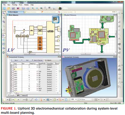
Multi-board 3D design environment. The new generation of ECAD systems offers a full multi-board 3D design environment. The mechanical enclosure can be imported directly into the layout, improving the chances for correct single or multi-board design. During layout, a wizard imports the 3D enclosure model and specifies all associated PCBs. Then, the PCBs are laid out with the enclosure in real-time, optimizing placement capacity and capturing interference violations earlier in the design process.
Interfaces with the leading MCAD systems make it possible to perform concurrent mechanical and electrical design. 3D parametric libraries are shared between the ECAD and MCAD systems. Electrical engineers can design to the true native 3D constraints as defined by mechanical engineers, while mechanical engineers in turn have access to the true 3D board design so they can accurately place and conduct interference checks during board layout. The STEP and SAT (ACIS) file formats are used to communicate 3D mechanical constraints and also to share real 3D electrical and mechanical components/assembly between ECAD and MCAD (Figure 3). Additionally, by importing accurate 3D enclosure and component models, engineers can create board outlines, design to the actual 3D enclosure as a constraint, and conduct interference checks to reduce data exchange and optimize multi-board floor planning and design. The new environment allows design teams to lay out complete system designs – from prototypes to complex, multi-board systems – using a single tool. Engineers and designers can flow through the design process optimizing form, fit and function of single and multi-board systems, maximizing design reuse, without reentering upfront planning data into the design tools during detailed design. Regular exchanges on board profiles for flex boards, bend lines and bend areas expand the level of detail and constraints that can be considered on the design.
Working with the exact product shape makes it possible to, for example, fit more functionality into the domed-shaped package of a pacemaker than could be accomplished with an orthogonal approximation. 3D ECAD design enables more accurate alignment of connectors so that they precisely fit openings on the enclosures. Electrical engineers can design multiple boards within a single model to ensure precise positioning of angles, shapes and cuts needed to avoid interference and to mate connectors. Rule checks support multi-board design for physical connector mismatches, I/O checks to ensure continuity between boards, and checks for duplicate references throughout the system.
Domain-level management. Finally, the latest ECAD systems provide domain-level management with metadata-based data handling at the file level, including explicit definition and tracking of object versions together with the controlled progression of changes through the development lifecycle. For development departments, this ensures that relevant changes are consistently highlighted and then distributed to all consuming models that require the change, even if the consuming models are located across many locations and sites. Change management support across the engineering process enables users to communicate individually with related teams, projects, designs, components or even across disciplines. It closes the loop on workflows by automatically notifying the relevant users or change groups and then provides them with acknowledgment and confirmation of the receipt of changes. History management capabilities perform concurrent changes to components throughout the product lifecycle, with full tracking and transparency.
Traditionally, mechanical and electrical/electronic design processes were separate, with design data being exchanged between MCAD and ECAD systems at critical stages. Limitations in the data exchange and lack of codesign functionality resulted in extra design iterations, driving up development time and cost. A native 3D ECAD environment opens the doors to breakthrough ECAD/MCAD collaboration. Electrical engineers can import a mechanical housing to a single or multi-board design and accurately place and conduct interference checks during board layout. The result is a reduction in design time, fewer errors and the ability to fit more functionality into a smaller package size.
Humair Mandavia is executive director of Zuken SOZO Center; This email address is being protected from spambots. You need JavaScript enabled to view it..
Three primary methods can be used, each with its pros and cons.
The question for this month’s column came from a conference call for an upcoming revision of IPC-2223, the flex circuit design standard. The discussion centered on sculptured conductors versus other methods of manufacturing unsupported fingers. It was soon apparent that many of the participants were not entirely clear on the differences among the variations. If there is confusion on this type of design from those who are fluent with flex circuitry, I have to believe that designers with less familiarity are even more stumped. This month I discuss the general concept of unsupported fingers, methods of manufacturing, and pros and cons of each flavor.
To begin, let’s review the general concept of unsupported fingers and the manufacturing methods used to create these circuits. An unsupported finger is a feature unique to flex circuitry. Figure 1 shows a flex circuit with unsupported copper fingers extending beyond the dielectric materials. These fingers can be used flat or formed, and can be soldered into plated through-holes or hot bar-soldered to a matching conductor pattern on a rigid PCB. There are three distinct manufacturing methods used to construct these circuits.
Method 1. The first method is to use pre-punched or laser-ablated widows in base and cover dielectrics. While the manufacturing processes are different for these two variations, the net result is the same. The oldest method of fabricating this variation is by pre-punching windows in the base dielectric prior to laminating copper foil. Identical openings are also punched in the top covers. After the circuitry is etched and covers laminated in place, any conductor crossing a window area will be unsupported.
The other way to construct this variant is to build the circuit as a normal flex, then laser-ablate the dielectric material from the window areas on both sides of the circuit, thereby leaving unsupported conductors. This type of circuit is the most cost-effective to manufacture, but can be a nightmare to ship, handle and assemble. Because the unsupported conductors will be the same thickness as the rest of the circuit (usually 1 or 2 oz.), they will be extremely fragile and easy to break. Designers will usually specify a “tie bar” of dielectric material be left along the outside end of the unsupported conductors. This tie bar will act to keep off the fingers aligned, and can be removed or left in place after connecting to the PCB. The most common method of connecting this type of circuit to a PCB is lap soldering to a matching conductor pattern on a PCB. It is imperative that the soldered area be over-coated with an epoxy because any mechanical force exerted on the circuit once soldered will break the fragile unsupported conductors.
Method 2. The second method for constructing this type of circuit is called sculpturing (shown in Figure 1). In this method, the manufacturer will start with a thick sheet of plain copper (typically 10 mil one-quarter or one-half hard copper). The copper sheet is selectively surface-etched to reduce the copper thickness by approximately 80% everywhere except the finger areas. The finger areas will remain full thickness. The balance of the processing is very similar to Method 1. The areas of the circuit that need to flex will be about 2 mils thick, but the fingers will be 10 mils thick, making them stronger than the first version. The downside is that the copper in the areas that need to flex will be one-fourth or half-hard rather than fully annealed. Using this type of copper will make the unsupported fingers stronger, but the circuit will not be able to withstand flexing, as well as one constructed from fully annealed copper. While the fingers in a sculptured circuit will be more robust than fingers made from 1 or 2 oz. copper, they will still be fragile and can be damaged easily if not handled properly.
Method 3. The final method of creating unsupported conductors involves adding fingers constructed from material such as nickel or full hard copper, and then welding or brazing the fingers to the flexible PCB. With this method, the circuitry is processed normally through etching, at which time windows are punched in the areas that will have the unsupported conductors. The fingers or tabs are then attached by welding or brazing the fingers to the matching pattern on the flex PCB. The balance of the processing is standard. This results in a flex circuit with fully annealed copper in the flexible areas and rigid fingers extending from the edge of the circuit. While this construction is the most robust of the three, it is also significantly more expensive and far from bulletproof when it comes to handling and assembly.
I would be remiss if I did not also discuss a variation on this theme that is well-established and popular. In this variation, insulation displacement contacts are crimped to the flex circuit at the very end of the fabrication. Insulation displacement contacts are very robust and tolerate handling better than any of the aforementioned types. They are also available from multiple vendors and can be ordered in a wide variety of terminal styles (Figure 2). The downside is that they add cost and limit contact pitch.
Assembling to a rigid PCB. The most common methods of joining the circuits described above with a rigid PCB are lap or through-hole soldering. Lap soldering can be accomplished either by hand or with a hot bar process. Unsupported fingers are simply positioned over a matching conductor pattern on a rigid PCB and then soldered individually (when done by hand) or all at one time (hot bar). When connecting flex to rigid using through-holes, the unsupported fingers are inserted into the matching hole pattern on the rigid PCB and soldered in place.
Each of these variations has its pros and cons, and designers should carefully weigh cost versus performance issues. As always, it is a good idea to discuss the options with your flex manufacturer.
Mark Finstad is a senior application engineer at Flexible Circuit Technologies (flexiblecircuit.com); This email address is being protected from spambots. You need JavaScript enabled to view it.. He and co-“Flexpert” Mark Verbrugge from PICA Manufacturing Solutions (This email address is being protected from spambots. You need JavaScript enabled to view it.) welcome your questions.