Where AOI and conventional x-ray peak, other methods can hone in on nettlesome defects.
X-ray and AOI, along with related equipment, have long been the stalwarts of post-placement printed circuit board inspection. Over the years, as packaging, device and board technologies have advanced, these inspection technologies have advanced as well to present the best inspection results possible based on the technology of the day. These inspection machines are nondestructive, meaning PCBs and their components remain intact while being inspected for failure analysis.
Certainly, even the simplest of inspection tools, the digital camera, with specialized lighting systems, continues to prove valuable for a number of tasks. Those include checking for cosmetic errors, verifying a component’s numbering system, viewing surface finish corrosion and half moons on the via sites, determining if the gold surface is peeling away from a board’s surface, whether the drill is properly controlled, viewing the dimples of delaminations, and a host of other potential problems. Some may be cosmetic in nature, but others could cause severe damage to the board.
Automatic optical inspection, programmed with the so-called golden (perfectly assembled) boards, compares that specimen with others that follow to capture design flaws or defects. It also catches defects such as wrong polarity, missing components, wrong components and incorrect orientation.
AOI continues to get smarter at catching board problems on the assembly floor. Newer generation machines have as many as six cameras, and offer side angle viewing of specific markings to observe components. State-of-the-art AOI comes with brighter LED lighting systems and, aided by software advances, captures a considerably better image and also detects greater numbers of accurate failures and fewer false failures.
In many cases, both conventional and automated x-ray inspection (AXI) are used on the assembly floor. AXI is used for leading-edge technologies such as ball grid arrays (BGAs), chip-scale packaging, flip chips, QFNs, DFNs, and others. It shines radiation through a component package such as a BGA to reveal whether balls are soldered properly to the PCB. Standard x-ray inspection is used for simple applications, whereas high-end x-ray is used to detect such tough-to-find defects as head-in-pillow, disjointed balls on a BGA package, wire bonding damage, and other similar problems.
These post-assembly inspection machines are precisely engineered for the tasks they are intended to perform. However, there exists one more hurdle to overcome given today’s design and technology demands: The current basic inspection issue or obstacle lies squarely on image processing. Image capturing is the easy part of the two; however, the biggest challenge is effectively capturing an image in low light. That’s not possible due to a high signal-to-noise ratio (SNR) in the design of current inspection systems. On the other hand, a lower SNR suppresses noise and increases and enhances an image. The challenge is for inspection system designers to suppress that excessive noise so that SNR is within acceptable limits.
However, today, with the rapidly escalating use of smaller, more complex packaging like µBGAs, µCSPs, and package on package (PoP), conventional inspection tools and their supporting technologies are finding it difficult to stay ahead of the demands smaller packaging and shrinking board sizes pose.
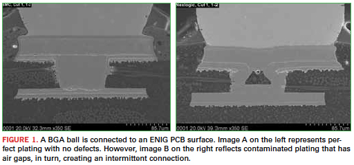
Consequently, the industry has to go deeper into these smaller PCBs and their small components to minutely strip away obstacles to view the tiniest of crevices to conduct failure analysis via forensics. For example, as shown in Figure 1, a BGA ball is connected to an ENIG PCB surface. Image A on the left represents perfect plating with no defects. Image B on the right reflects contaminated plating that has air gaps, in turn, creating an intermittent connection.
[Ed.: To enlarge the figure, right-click on it, then click View Image, then left-click on the figure.]
The absence of forensic analysis tools and techniques puts ample time (rework and product delays) and money (in labor and materials) at risk.
In response, conventional nondestructive inspection is partnering with forensics analysis to do detective work and sleuth around the insides of a package on package (PoP), for example. This newest of inspection techniques is increasingly making its way into the assembly floor with its bag of tools to investigate and detect the smallest of culprits causing board defects. The tools include scanning electron microscopy (SEM) and time domain reflectometry (TDR). While this technology isn’t exactly new, some service bureaus use it to specialize in this type of failure analysis. Forensics isn’t in the mainstream of PCB assembly today, but it’s making inroads.
Board Sacrifice
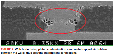
With forensic analysis, more commonly known as destructive inspection, one board from a project order that is demonstrating poor performance is sacrificed for what is essentially an electronics autopsy. That board and the devices populating it are dissected, and extremely high electron microscope magnification views physical cross-sections in pursuit of the problem. For instance, in the case of buried vias, plated contamination can create air bubbles to be trapped between walls of the via, thus creating intermittent connections (Figure 2) that otherwise could not be revealed by conventional inspection.
Forensics analysis comes in at a time when conventional inspection cannot locate the problematic areas. Say x-ray, AOI and specialized high megapixel digital cameras are in use, but yields are below acceptable levels. You’re absolutely sure of your processes, the different flow charts, and of manufacturing. However, you’re not able to pinpoint a certain defect. That’s when forensics comes into play.
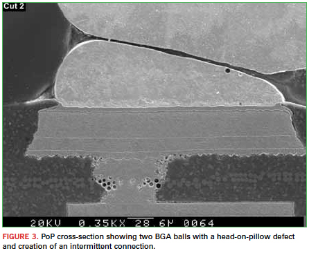
Again, take the PoP as the example. It’s not performing or is failing. The pass rate and yields are extremely low. Here, the cross-section of this PoP plays a central role in failure analysis. It provides physical evidence and root cause of the failure mode, shows the failure site location, and then isolates it from suspected versus non-suspected devices. Figure 3 shows the cross-section of a PoP. Two BGA balls are shown with a head-in-pillow defect, another cause for an intermittent connection.
Forensic analysis uncovers an innumerable number of defects or failures that conventional inspection cannot. At the board level, it investigates thickness of copper plating on the through-holes and vias; if it’s an immersion gold finish, the gold plating thickness can be observed to determine whether an adequate amount of gold has been deposited, per fabrication specs. On an electroless-nickel immersion gold (ENIG) finish, forensic analysis ensures the nickel, which is the base plating before the gold is deposited, is performing according to the spec sheet. Also, it pinpoints infinitesimally minute fractures within solder joints.
Minute solder pinholes are not visible at the 300X to 400X magnification level. But with SEM, those pinholes are magnified upwards to the 2,000 times level. Plus, in some instances, black pads, the acute corrosion of a board’s nickel-plating layer, can be viewed very clearly. Moreover, one of the more elusive issues, particularly with BGAs and µBGAs, is the problem with intermittent connections, meaning a faulty connection between and among a BGA’s balls exists. Forensic analysis can locate these inter-metallic failures, which are the most troublesome when it comes to BGAs in systems out in the field. It can determine the distance between gold plating and the solder ball, in case BGA balls are detached after the assembly process, and also comes to a conclusive analysis when checking organic solderability preservative (OSP) versus gold versus immersion silver board surface finishes.
Solder thermal fatigue and current leakage failures are other specialties forensics excel in. Due to solder thermal fatigue, open circuit failure occurs in the field when a product is subjected to excessive heat, rugged conditions or extreme temperature variations, especially on BGAs or PoP devices. Those defects are especially prevalent in PoP packages because multiple BGA devices are stacked on top of each other, and that process needs to be 100% accurate or else it will create field failures. Those fatigue cracks become more pronounced over time. A solder joint experiencing those cracks eventually detachs from the board’s surface due to the excessive heat. This is especially true if the BGA is not properly assembled.
In some instances, solder bridging of flip-chip devices has leakage failures. After thermal cycling, the device leaks current due to solder or flux; insufficient current arrives at a BGA’s proper ball, and an unacceptable signal is then provided at certain levels. This especially occurs when underfill is used between a solder ball and board surface.
The data developed via forensic methods can then be fed upstream to the designer to respin the board, as necessary.
If quality assurance reveals persistent PCB problems that otherwise cannot be resolved by tweaking the AOI, forensics are the next step to revealing the source of the defect.
Zulki Khan is president and founder of NexLogic Technologies (nexlogic.com); This email address is being protected from spambots. You need JavaScript enabled to view it..


