Inexpensive, high-performance packages can be fabricated by
laminating thin, flexible, mechanical devices into conventional
multilayer circuit boards.
The packaging industry and the research
community are developing new techniques for keeping up the race for
increased functionality in smaller packages, and 3D integration is a
good option in this respect. One 3D approach, the integration of active
circuits inside the innerlayers on a multilayer rigid or flexible
printed circuit board (FPCB), allows for a high degree of
miniaturization. Recently, an ultra-thin-chip package (UTCP) technology
was worked out, which allows embedding thin dies inside these flexible
circuits.
Today’s rapid succession of new cell phone
iterations clearly illustrates the mission of the electronics industry
to increase functions while decreasing the size and weight of
electronic products. The semiconductor industry meets this target by
miniaturizing transistors to integrate more of these building blocks
onto the same silicon area. The packaging industry, on the other hand,
is challenged to integrate and to shrink the IC and system’s package.
There
are a number of packaging technologies that have been developed and
deployed to reduce the footprint of IC and system’s packages: flip chip
bonding instead of wire bonding; chip-scale packages; and
system-on-chip and system-in-package technology.
Using the Third Dimension
For
some applications, the technologies described above are still not
sufficient to meet the product requirements. For example, think of
third-generation PDAs with telephones, internet, GSM and photographic
capabilities. To increase capacity and/or functionality in the same
volume, 3D packaging methods are required.
There are different
approaches for 3D modules. Multiple dies can be stacked inside a
package. Aside from space savings, die stacking also results in better
electrical performance of the device, since the shorter routing of
interconnections between circuits results in faster signal propagation
and reduction in noise and cross-talk. The stacked die may be
interconnected using wire bonding alone or by a combination of wire
bonding and flip chip assembly. Alternatively, through-silicon vias
(TSV) can be used to interconnect the stacked dies, allowing for
further miniaturization and increased performance.
A second 3D
approach is the use of stacked packages. In this case, the 3D stack
consists of subunits that are assembled after package level burn-in and
test. The advantages offered by the package-on-package (PoP)
architectures include memory flexibility and easy testing compared to
application specific integrated circuit (ASIC) and memory die stacking,
as well as the ability to mix and match devices from multiple vendors.
A
third approach for stacking active devices is the technique of folding
stacked dies to eliminate the need for spacers between them. This
process is referred to as “folded/stacked” technology. The dies are
produced side-by-side and then folded over so that the bond pads are
independent of each other. A relieving layer is placed between the
chips to alleviate thermo-mechanical stresses.
Finally, the 3D
approach with the highest level of miniaturization is the integration
of ICs inside circuit boards. The assembled packages, with active
circuitry, are thus removed from the outer layers of the substrates
and, together with passive components, are incorporated inside the
circuit board. The complete product or system, including numerous
passive and active components, can then be integrated inside the
motherboard, producing a System-In-Board (SIB) product. Such modules
allow assembly of surface mount devices on the bottom and top surface
and are typically used as motherboards for the rest of the components.
Some
technologies are already developed for integrating bare dies in the
innerlayers of multilayer substrates. Examples include the
Chip-in-Polymer technology (CiP), the chip-in-substrate package (CiSP)
and the Integrated Module Board technology from Imbera Electronics.
These above-mentioned technologies integrate the bare dies directly
inside the substrates. Possible hurdles include testing of the dies
before embedding (Known-Good-Die problem), necessary precise placement
of the bare die and the need for a very fine pitch PCB or FPCB,
compatible with the pad pitch of the embedded chip.
Recently,
Belgian researchers from IMEC and the Ghent University developed an
alternative approach for integrating ICs in PCBs and FPCBs: the
ultra-thin-chip package (UTCP) technology, which permits testing of the
chip before embedding and provides a contact fan out with a more
relaxed pitch. This eliminates the need for precise placement and
ultra-high-density PCBs.
UTCP Process Flow
UTCP technology
is a polyimide-based embedding technology for integrating very thin
silicon chips in flexible substrates. Dies with thicknesses down to
15μm can be embedded between two 20-μm-thin, spin-on polyimide layers,
resulting in a package with a total thickness of only 50 μm to 60 μm.
Thanks to the very low thickness of the chip, the polyimide layers and
the metal, the whole package is bendable.
The base substrate
is a 20-μm-thick polyimide layer, spin-coated on a rigid glass carrier.
For the fixation and the placement of the chips on the polyimide layer,
a benzocyclobutene of about 5 μm is used as adhesive. By placing chips
properly in a dispensed benzocyclobutene, void-free bonds can be
obtained. After the cure of the benzocyclobutene at 350° C, the chips
are fixed on the polyimide layer. A covering polyimide layer is
spin-coated on the fixed die with a layer thickness of about 20 μm.
This allows the chip to be embedded between the two polyimide layers.
For interconnecting the chip, contact openings to the bumps of the
chips are laser drilled. Next, a top metal layer of 1 μm TiW/Cu is
sputtered and photolithographically patterned, metallizing the vias to
the chip and providing a fan out to the contacts of the chips. If
needed, the sputtered top metal layer can also be enforced by
electroplating. Finally, after processing and functionality testing of
the integrated devices, the whole package can easily be released from
its rigid carrier. The process flow can be seen in
FIGURE 1.

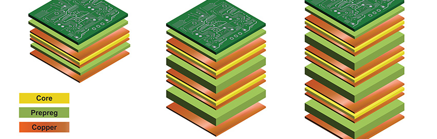
Embedding for Flexible Circuits
Flexible
circuit boards can be used to integrate electronics into clothing or
onto curved surfaces such as machine parts. On typical flex substrates,
only pure electronic assembly is performed on the flip chip components.
Embedding of passive or active components in flexible printed circuits
is not state of the art. The presence of relatively large rigid
components, only on the front and backside of the flex laminate, is an
important factor limiting not only the miniaturization, but also the
mechanical flexibility of the circuits.
Based on the
above-mentioned UTCP approach, a technology was worked out for the 3D
integration of active devices inside the innerlayers of commercial
multilayer flexible circuit boards (
FIGURE 2). The UTCP packages
serve as interposers: ultra-thin active devices are first integrated as
UTCP, which in turn, is embedded inside a standard multilayer flex
circuit.

A suitable process flow to
integrate small UTCP packages inside large flex laminates has been
successfully established at ACB, a Belgian flex manufacturer. UTCP
packages are aligned and fixed (by heat tack) on a patterned inner
layer of the multilayer substrate, and connection between package and
wiring of the PCB or FPCB is achieved by through-hole interconnects.
This
embedding concept was first demonstrated with UTCP test packages,
indicating that a 3.5 μm metal thickness on the UTCP package is
sufficient to ensure good interconnects and that an ENIG metal finish
on the UTCP samples will not affect the through-hole plating quality.
Daisy chain interconnects between integrated dummy packages and the
FPCB were characterized and monitored during reliability
investigations. High temperature storage at 150° C (up to 1000 h), hot
humidity storage at 85° C/85 relative humidity (up to 1000 h) and
thermal cycling between -40° C and +125° C (up to 1000 cycles) did not
introduce any failure at the interconnects. The integration process
also does not affect the values of the 4PT via resistance of the
interconnects on the UTCP package.
Technology Demonstration: Functional ECG
Wearable
monitoring systems for health or sport applications often make use of
flexible circuit boards. In this way, they can unobtrusively be
integrated into clothing or be worn in the form of a ‘band-aid’. An
important factor limiting miniaturization and flexibility is typically
the presence of relatively large rigid components. For this reason, the
UTCP technology for embedding active circuitry into an FPCB is ideally
suited for these systems.
A prototype ECG/EMG wireless monitoring system (
FIGURE 3)
was realized using the above-described technology. The prototype
measures the heart rate (electrocardiogram or ECG) and muscle activity
(electromyogram or EMG). It consists of three integrated circuits: an
ultra-lowpower ECG/EMG amplifier circuit, a commercial TI
microcontroller with embedded analog-to-digital converter (ADC) and a
Nordic 2.4 GHz low-power radio transceiver. Additionally, some
supporting passives, a battery, a loop antenna and some electrodes are
included.

The microcontroller and ADC
circuit were embedded inside an FPCB. First, the individual chip was
thinned down, starting from the initial die thickness of 300 μm to 25
μm, using a proprietary-developed individual chip thinning process.
Secondly, these very thin, functional microcontroller devices were
embedded as an ultra-thin-chip package. The UTCP-packaged
microcontroller could easily be tested after assembly but before
release from its carrier. After testing the UTCP-packaged
microcontrollers, they were cut out from the glass substrates,
resulting in ± 1 cm² x 1 cm², square UTCP packages. Next, the
UTCP-packaged microcontrollers were integrated in the innerlayers of
the multilayer flex substrates. Finally, components were assembled on
both sides of the flex substrates: SMT components, the IMEC
biopotential ASIC and the Nordic radio. These actives were wire bonded
on the substrates (Chip-On-Flex, [COF]), after the SMT components were
assembled.
The wireless ECG/EMG biopotential prototype (
FIGURE 4) with UTCP-packaged and FPCB-embedded microcontroller (
FIGURE 5) proved to be completely functional and able to monitor ECG and EMG signals.


Conclusion
The
ultra-thin-chip package (UTCP) technology offers the possibility to
integrate functional devices inside flexible multilayer circuit boards.
These UTCP interposers provide a contact fan out with more relaxed
pitches, allowing for easy testing before integration. Moreover, this
fan out eliminates the need for precise placement and
ultra-high-density printed circuit boards. The thin, mechanical
flexible devices can be laminated inside the adhesive innerlayers of
conventional low-cost multilayer substrates, using only standard
production processes. PCD&F
ACKNOWLEDGEMENTS
This
research was done in the framework of the FP6 project SHIFT. This
publication is intended to report the outcome of the research and the
capabilities of the technology developed in the framework of this
project.
Els Parton is a scientific editor responsible
for authoring and editing IMEC’s company technical documents and
publications;
This email address is being protected from spambots. You need JavaScript enabled to view it..
Wim Christiaens is a technology developer at Ghent University.
Jan Vanfleteren is a senior engineer with the IMEC-CMST group and a part time professor at the Ghent University.