A low-cost solution for flexible circuits can be manufactured using silver conductive paste and screen-printing techniques.
In the past, polymer thick-film circuits have been used primarily for single-sided circuits with low circuit densities. Traditional polymer thick-film materials have lower conductivity and insulation capabilities when compared to standard copper foil laminates. This limitation is unfortunate because the screen-printing process using silver paste to additively form circuits can provide a simple and low-cost solution for electronics manufacturing.
There have been many technical improvements with ink materials and within the screen-printing process1 that are now enabling additional circuit processing capabilities for not only fine-line generation, but also multilayer capabilities with new via hole manufacturing techniques. These improvements have been incorporated into the Advanced Screen Printing (APS) process. In addition, two types of via hole forming processes have been developed: one for double-sided and a second for multilayer thick-film circuits, both formed on thin flexible substrates.
Punched Via Holes
The first via hole process is based on the through-hole process for traditional double-sided flexible circuits.
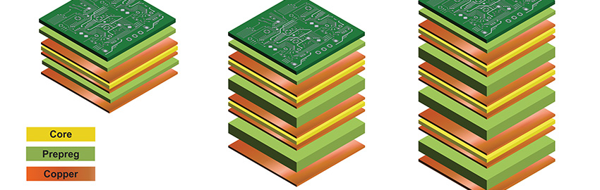
FIGURE 1 indicates the layer constructions of the via hole technologies. The through-hole structure of the thick-film flexible circuit made by the APS process is much simpler compared to the traditional copper foil process that uses photolithography, copper etching and copper plating. There are more differences in the manufacturing processes, as shown in
FIGURE 2 and
FIGURE 3.


Figure 2 does not show details of the process, such as lamination of the copper foil, surface cleaning or development; therefore, the total steps of the process are more than a dozen. Many of these processes need long rinse times and lengthy equipment. Additionally, the wet processes produce large amounts of chemical waste. Accordingly, a relatively large investment is required to build the whole manufacturing process, and processing materials, such as plating chemicals, etching resist, etching solution and stripping solution, are additional costs. They are the major reasons why the cost of the double-sided flexible circuits is more than twice that of a single-sided product.
On the other hand, the manufacturing process for thick-film flexible circuits with through-holes is quite short and simple. There are several processes that can be used to generate the holes in the flex film including: laser drilling machines, NC drilling equipment and NC punching machines. The latest UV laser machine can produce holes smaller than 50 micron in diameter, with speeds greater than 200 holes per second in thin polyimide films. The latest NC micro punching machine can produce holes down to 50 micron. Both laser and punching machines can be operated in a RTR (roll-to-roll) format for high-volume production.
Simple screen-printing processes, followed by drying and baking, are conducted to form double-sided thick-film flexible circuits with through-holes. The final screen-printing that fills the holes with silver paste can be eliminated by appropriated hole sizes. The holes are filled with the silver paste during the trace printing process.
The APS process needs only a screen-printer, a thermal oven and equipment to drill holes. No facilities are required for waste treatment, because there is no wet process. The total investment for manufacturing thick-film flexible circuits can be remarkably smaller compared to the manufacturing process of standard copper foil circuits.
Printed Via Holes
The advanced screen-printing process has another choice to generate printed via holes for double sided and multilayer flexible circuits, as shown in
FIGURE 4 and
FIGURE 5.
The printed via hole process is simpler than that for through-holes requiring specific hole-generating equipment. Manufacturing costs can be much less because the drilling process requires less investment. The via hole size depends on the screen-printing capability of the insulation layer. Currently, the minimum hole size cannot be smaller than 300 microns in diameter because of the resolution limitations of the screen-printing. The big advantage of printed via holes is the multilayer capability that can be achieved by building layer-on-layer of circuitry and insulation, as shown in Figure 5.


Several daisy chain patterns have been generated for the reliability test of the through-holes and printed via holes on the flexible substrates.
FIGURE 6 shows one of the examples. It has a 150-micron diameter pad, assuming holes smaller than 100 microns in diameter with high accuracy alignment.

Thick polyimide films (50 micron) and PEN films have been employed for the reliability tests. RTR micro punching was used to generate small holes on the thin films down to 80 microns in diameter. Using a high conductivity silver paste, the ASP process was followed and repeated to form two-layer circuits for both sides of the thin flexible substrates. The two-step screen-printing could make reliable through-holes without the hole filling process. The screen printer used for the test has an automatic alignment mechanism for accuracy better than +/- 20 microns. The through-hole generation yield was determined to be higher than 99.9% for the 150-micron diameter through-hole pads made on the thin flexible films.
FIGURE 7 shows the cross section photo of the through-hole built on a 50-micron thick polyimide film. The 80-micron diameter hole was filled with the silver paste by screen-printing twice. The resistances of the through-hole connections are almost negligible compared to the resistances of the printed conductors. The calculated resistances of the through-holes are smaller than 20 milliohms per hole.

The printed via holes with 500-micron diameters were built on both polyimide and PEN films. The traditional screen-printing process formed epoxy resin insulation layers, 10 microns to 15 microns thick.
FIGURE 8 shows an example of the test pattern made on a polyimide film. The resistance of the via holes are negligible compared to the printed thick-film conductors. The estimated via hole resistance could be smaller than 20 micro ohms with better than 99.9% yield.

Multilayer Capabilities
Further trials and considerations were conducted for the multilayer constructions of thick-film flexible circuits. The simplest way to build more layers is to repeat the printed via hole process shown in Figure 5. However, it may be difficult to keep the flexible circuits flat when layer counts are greater than four because of the extreme imbalance in the construction. Suitable combinations of the drilled via holes and printed via holes built on both sides of the thin flexible substrates are preferred, as shown in
FIGURE 9.
 FIGURE 10
 shows an example of the multilayer test pattern that was built on both sides of thin flexible polyimide films using a combination of punched via holes and printed via holes. The via hole yield during the manufacturing process is better than 99.9%.

An advantage with the ASP process is that additional layers can be produced for only the necessary portions of the flexible circuits. This is valuable when building multilayer flex or rigid/flex, as shown in
FIGURE 11. A complicated multilayer construction can be built by only repeating the conductor layer and insulation layer screen-printing where it is needed.
The process concept is suitable for building embedded passive components on thin flexible substrates.
FIGURE 12 illustrates an example of the trials. All of the resisters, capacitors and inductors were built on a three-layer, thick-film circuit with punched via holes and printed via holes. The simple process of screen-printing with drying/baking was repeated more than eight times to make this construction.


Conclusion
The trials of the ASP process have shown a broad range of capabilities when building multilayer constructions on thin flexible substrates. This alternative process technology provides low-cost solutions when compared to traditional copper foil circuits made by a photolithography, etch and plate process.
PCD&FREFERENCE
“Advanced Screen Printing Process–Practical Approaches for Printable & Flexible Electronics,” Dominique Numakura, 3rd IMPACT and the 10th EMAP, Taipei/Taiwan, October 2008.
Hhisayuki Kawasaki (
This email address is being protected from spambots. You need JavaScript enabled to view it.) and
Masafumi Nakayama (
This email address is being protected from spambots. You need JavaScript enabled to view it.) are both with NY Industry.
John Rufiange (
This email address is being protected from spambots. You need JavaScript enabled to view it.) and
Dominique Numakura (
This email address is being protected from spambots. You need JavaScript enabled to view it.) are with DKN Research.