Catching excessive noise can be all about timing.
Electromagnetic compatibility (EMC) compliance is a necessary condition for releasing products to market. National and international standards bodies such as the Federal Communications Commission (FCC) and the International Electrotechnical Commission (IEC) define limits on the radiated and conducted emissions that a device is permitted to produce. Automotive and aerospace manufacturers can set even stricter standards for their suppliers. Simply stated, if a product does not pass EMC compliance testing for the target market, then the product cannot be sold.
Design teams are well aware of the importance of ensuring their product is EMC compliant. Many, however, do not attempt to perform EMC analysis during design. There is a perception that EMC analysis during PCB layout can be a time-consuming task that is challenging to set up and properly configure, with difficult-to-interpret results.
Historically, the focus of analysis during design has been on signal integrity (SI) and power integrity (PI), with EMC “analysis” performed manually post-fabrication based on the results of testing the actual product. What is often overlooked is that automated EMC analysis during the design phase provides an opportunity to avoid failing EMC compliance testing after fabrication.
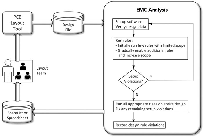
The current generation of ECAD tools offers EMC analysis functionality that is easy-to-use, with well-documented rule checks that often include an explanation for each principle and advice on how to address issues. Adding EMC analysis at appropriate points during PCB layout, prior to fabrication, can mitigate the need for redesign(s) that impact both product development cost and overall time to market (FIGURE 1).

Figure 1. EMC analysis during PCB layout.
EMC can be a daunting and confusing topic, especially for new engineers and designers, or those not well-versed in the subject matter. There is often confusion as to the difference between electromagnetic compatibility (EMC) and electromagnetic interference (EMI). Although this article is not intended to be an in-depth tutorial on EMC and EMI theory, a quick review of the definitions is appropriate.
EMC is generally defined as the ability of a product to function in its environment without introducing electromagnetic disturbance. Specifically the product must:
- Tolerate a stated degree of interference.
- Not generate more than a stated amount of interference.
- Be self-compatible.
EMI is generally defined as a disturbance that affects an electrical circuit due to either electromagnetic induction or electromagnetic radiation.
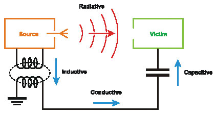
To further simplify the two definitions, EMC is how vulnerable the product is to the environment, and EMI is what the product introduces into the environment (FIGURE 2).

Figure 2. The four basic EMC/EMI coupling mechanisms relative to the source and victim.
The complexity of the topic contributes to the perception EMC analysis during PCB layout can be a time-consuming task that is challenging to set up and properly configure, with difficult-to-interpret results. Yet the alternative – foregoing automated in-design analysis and waiting to test the actual product post-fabrication – has the potential to be significantly more time-consuming and costly. Although EMC test labs are not required to provide the average EMC testing pass rate, several studies suggest the first-time pass rate is approximately 50%. Further, EMC compliance failure has been cited as the second-leading cause for redesigns in the automotive industry. Given an EMC failure will require one or more redesigns that impact product development costs and overall time-to-market, performing EMC analysis during PCB layout (designing for EMC compliance) is essential.
Analysis ‘Shift’
In the engineering space the term “left-shift” is often used to describe the act of moving (or shifting) a task from the latter phase of the design process to an earlier phase in the design process. Generally speaking, shifting the task does not necessarily eliminate the need for the task later in the process; rather, it is intended to both reduce the dependency and improve the result. In this case, EMC analysis that will be performed based on the results of post-fabrication EMC testing will be shifted, and also be performed using an integrated solution executed at appropriate points during the PCB layout phase. The goal of left-shifting is to provide an opportunity for engineers and designers to perform tasks earlier in the overall design process, ultimately eliminating iterations and ensuring the overall flow is more efficient. Fundamentally, each time analysis is performed during the various phases of PCB layout, the overall design process improves. The greater the degree of the shift applied, the greater the benefit (FIGURE 3).

Figure 3. Left-shift of EMC analysis.
Consider the typical use case. Traditionally, an engineer or designer will perform some simplistic manual EMC analysis within the PCB design system, but will then rely on the results of post-fabrication EMC testing to determine if more detailed analysis is required. In this external, post-design analysis environment, any EMC problems that are detected must be passed back to the designer for corrective action. Once the first set of changes are made to resolve EMC issues found during testing, a new design must be fabricated, and the cycle starts over again. There is also an assumption that the details of any EMC issues found during testing can be analyzed and communicated in such a way that they can be resolved in the PCB design system. The validity of this assumption will vary based on the level of expertise of the EMC test lab. Manual inspection for EMC issues is not only time-consuming; it is also subjective and has the potential to be inaccurate and error-prone. By left-shifting EMC analysis to an automated in-design process, the cycle time of determining and resolving EMC issues is no longer subject to outside influence. The closer the analysis is to the engineer or designer, the more often it will be run, and the easier it will be to detect and correct issues earlier in the design process.
Early and often. Given that a single design improvement can often reduce both EMC emissions and susceptibility, analysis run early and often at
appropriate phases of the PCB layout can provide significant benefit. Many design teams spend significant effort to contain potential EMC/EMI issues, rather than investing time to use analysis to suppress them instead. As mentioned, the current generation of ECAD tools includes functionality that can perform various EMC and EMI rule checks against both placement and routing to support optimal layout design. In the best-case scenario, the ECAD tool used for PCB layout will provide EMC analysis functionality where:
- Every rule is well-documented.
- Each rule’s principle is explained.
- Examples that include diagrams are provided, detailing any setup required.
- Advice is provided on how to correct issues.
Some examples of issues that can be checked for during embedded EMC/EMI analysis include:
- Stub length.
- Filter placement.
- ICs over split planes.
- I/O coupling.
- Copper islands.
- Nets near plane edge.
- Traces crossing plane splits.
- Traces referencing wrong voltage.
- Via stub length.
In each of these examples, the user does not need to have in-depth knowledge of EMC/EMI rules in order to run the automated analysis.
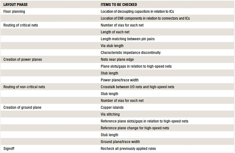
TABLE 1 is an example of items that should be checked using EMC analysis during various phases of the PCB layout. Notice that in some cases the same item will be checked during more than one phase of layout. This does not imply checking the same parameter twice, but rather that, as the design progresses, analysis may need to be repeated. For example, consider the maximum number of vias for a net. The results of an analysis after the routing of critical nets may change later in the design cycle, after power and ground planes are added, along with non-critical nets.
Table 1. EMC/EMI Items to be Analyzed During Each Design Phase
EMC analysis results can be extremely accurate with cross-probing from the results to the layout and advice on how to correct an issue. The basic rules usually do not require any setup. For more advanced rules, however, usually some setup is required. As such, the results will be somewhat dependent on the design team’s EMC expertise.
Summary
The pinnacle achievement for most engineers and designers is to produce a system that works reliably at full speed and is still quiet enough to pass EMC compliance tests without expensive shielding and filtering, and to do so during the first fabrication. Achieving electromagnetic compatibility is a significant design milestone. EMC analysis that is left-shifted and embedded into the PCB design tool can greatly reduce the potential for EMC compliance failure after fabrication. Embedding of the analysis should not be a single event but rather a series of events that occur at appropriate phases of the PCB layout to help guide the engineer and designer toward a more EMC-correct physical implementation. This direct relationship between engineer and analysis means critical design decisions to support EMC compliance can be applied at each phase of the PCB layout process. Each time a left shift in the EMC analysis is applied to the PCB layout process, there is a gain in efficiency. The ultimate goal of any left-shift program is to permit the design system to support a correct-by-construction methodology using EMC rules to eliminate costly post-design iterations.
To summarize, adding automated EMC analysis to PCB layout has multiple benefits, including:
- Designing an EMC-correct physical implementation.
- Reducing the dependency on post-fabrication EMC analysis.
- Improving the probability of passing EMC compliance testing during the first fabrication.
- Automating a subjective, time-consuming and potentially error-prone manual process.
- Reducing or eliminating rework late in the design cycle.
These benefits are just the beginning of what can be realized. As with any new technology, transformation will most likely occur in stages. Initially, design teams may just focus on a few select basic rules that are the most critical, or most subject to error or misinterpretation. As design teams become familiar with the latest generation of embedded EMC rule checks, they will most certainly also work to enhance their processes over time, resulting in improved timeliness, accuracy and quality of the associated products. The goal is continual process improvement. In the end, automated EMC analysis embedded into PCB layout is a win for both the product development team and the manufacturing team, with improved quality, reduced costs, and improved time to market.
Craig Armenti is a PCB marketing engineer at Mentor (mentor.com); This email address is being protected from spambots. You need JavaScript enabled to view it..


