Optical and SEM images of real-life soldering problems reveal specific features identifying the condition.
Some solderability issues can be seen and inspected, and some are hidden from view under components. Visible problems include tombstoning of small components, missing components, shorted pins or lifted pins in gullwing components. BGAs and QFNs (quad flat no leads) hide their soldering issues well, requiring x-ray inspection. Shorts are relatively easy to detect, but open pads in QFNs and cracked balls or head-in-pillow (HiP) balls in BGAs are not always detectable. In 2-D x-ray often components of the other side of the substrate can hide the region of interest.
Many techniques are available, each with strengths and weaknesses. X-ray imaging detects solder bridges, missing solder and voids, but is not so good at detecting cracked solder (FIGURE 1). Acoustic microscopy detects delamination inside a component and bowing but cannot see a cracked BGA ball because the BGA substrate has too much absorption. Failure analysis techniques are good at detecting excess current because that generates heat or light. When it comes to opens, since there is no signal, there is no telltale signature. One needs to resort to electrical tests for continuity if possible, or do dye and pry or cross-sections, which are both destructive. SQUID (superconducting quantum interference device) analysis is very expensive and difficult to interpret.
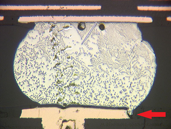
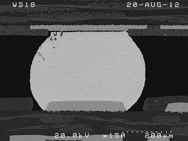
Figure 1. a) Cross-section optical image of a ball separated on the board side. The viewing direction for optical microscopy (before cross-section) is indicated by the arrow. b) Cross-section SEM image of a ball separated on the component side.
In Figure 1a, along the edge of the package, the solder wraps around the edge of the solder pad, hiding the crack from view. Meanwhile, in the cross-section SEM image in Figure 1b, even if optical inspection had been possible, the crack is hidden by the solder mask. Encapsulation epoxy has been used to prepare these parts for cross-section. The epoxy expands during curing, opening existing cracks. Before encapsulation, the cracks were most likely closed, remaining hidden to x-ray examination.
Black pad is a corrosion of the surface of the Ni layer during gold plating in ENIG (electroless nickel immersion gold).1 This causes the growth of a thin Ni3P layer, which prevents formation of the intermetallic layer during soldering. The consequences are poor wetting and a weak solder joint. The corrosion can be uneven across the board, with areas more affected than others. Black pad is recognized before soldering or on pads with separated solder joints by characteristic mud cracks visible in SEM imaging or by cross-sections and high-magnification imaging.
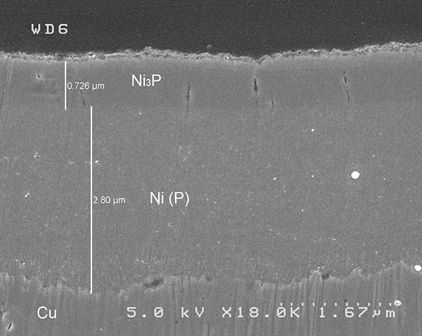
Figure 2. Cross-section of solder pad affected with black pad. The Ni3P layer is less than a micrometre thick and shows cracks.
Black pad is often detected as a root cause after assembly when failures occur. Yet there is no need to wait for the “autopsy” before the diagnostic of a “disease” is done. The characteristic signature of black pad is visible on a bare board. Although boards with black pad cannot be “cured,” they can be removed, avoiding the expense of an assembly doomed to failure.
Black pad on bare boards. In extreme cases black pad gives a dark appearance to solder pads, hence its name. When exposed to a humid environment, nickel corrosion can progress and cause blistering on the pads (FIGURE 3).

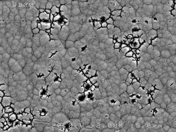
Figure 3. Black pad affected board exposed to humidity. a) Optical cross-section image across a blister bubble. b) Plan-view SEM image of another region of the same part. Mud cracks are very visible in SEM because they are coated with the ENIG gold plating layer. They are also visible in the optical cross-section, once one is acquainted with their appearance. The blue arrow in (a) points to such a crack.
The main issue with optical microscopy is the lack of depth of field at high magnification. A small tilt or curvature of the sample and focus is lost. It has the advantage, on the other hand, of showing colors. In SEM imaging, there is very poor contrast between Cu and Ni, but depth of field is not an issue. Mud cracks do show well, as seen in FIGURE 4, but they are very small and can be missed if one does not know what to look for.

Figure 4. SEM cross-section image of a board affected by black pad. A string of mud cracks is visible at the interface between the gold layer and nickel. They have the appearance of little black dots at this magnification.
Black pad after solder. When small components fall off a board at the slightest touch, the culprit is often black pad. In the example shown in FIGURE 5, there is very poor wetting of the solder on the pad under the capacitor, and where the capacitor has fallen off, there is no solder left on the pad. X-ray imaging of the pads of fallen components is a rapid way to check if black pad is involved.
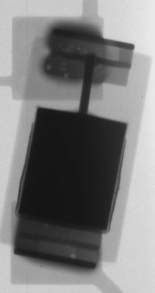
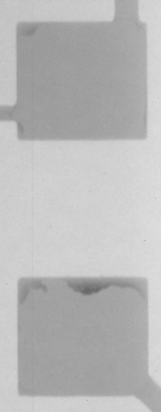
Figure 5. Left: X-ray image showing poor solder wetting of a tantalum capacitor. Right: Area where the capacitor has fallen. Most of the area of the pads is clear of solder.
When a part falls off, one is not tempted to take an x-ray of the region; yet it may provide valuable information on the failure mechanism if the path is clear of interference from components on the other side.
BGAs do not usually fall off when cracked balls are suspected. Dye and pry is a common technique to assess the number of bad balls. Detailed examination of the failed solder pads indicates whether the problem was black pad or some other mechanism (FIGURE 6). Mud cracks are present overall, and there are small clumps approximately 10µm across (red arrow, Figure 6c). These are small regions of intermetallic formation. Energy dispersive x-ray (EDX) analysis of the mud crack region reveals a high level of phosphorus, attributed to the formation of the Ni3P layer at the nickel surface.
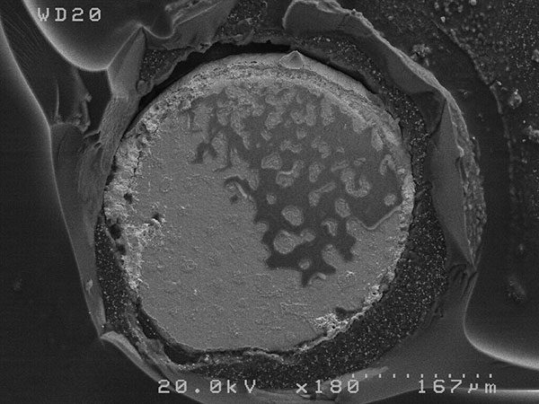


Figure 6. a) SEM image of a board pad after dye and pry test. Approximately half the pad is covered with dye (darker region). The rest of the dye adhered to the solder ball during the pry. b) SEM image of the partially dyed solder ball remaining on the component after dye and pry. c) Higher magnification image of the light region on the board pad.
In solder joint cross-sections, in addition to mud cracks, one sees the intermetallic layer is not uniform in parts affected by black pad (FIGURE 7). Note the SEM images in Figure 7 were taken with a 20kV acceleration voltage, and that of Figure 2 was taken at 5kV. Hence the appearance of the layers is different. FIGURE 8 shows optical images of the same parts as Figure 7, which is proof an electron microscope is not needed to confirm black pad.
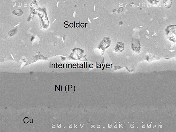

Figure 7. SEM cross-section images of a) a good board and b) a board affected by black pad. On the bad board, the intermetallic layer is not continuous, and the mud crack affected Ni3P layer has formed on top of the nickel.


Figure 8. Optical images corresponding to the SEM images in Figure 7. There is no intermetallic layer on the bad board.
Other solder failures. Black pad is not the only mechanism causing solder cracks, and one needs to recognize the morphological signature of the root cause. Board flexion (FIGURE 9) can also cause cracks, and such cracks are often found at opposite sides of the ball. They are usually very sharp following grain boundaries and occur in or near the intermetallic.

Figure 9. Example of a flexion crack in a BGA ball.
Coefficient of thermal expansion (CTE) fatigue also causes solder cracks, but those have a different morphology. In FIGURE 10, the cyclical heating and cooling of the part causes phase separation in the solder, creating a weaker area where the crack occurs. Figure 10a (top) is an optical image showing the contrast of the different phases. The solder has started cracking on the right. Figure 10b (bottom) is a SEM image of a nearby pin where the crack has propagated.


Figure 10. Examples of a CTE solder cracking event. In the top image, the solder has started cracking on the right. The SEM image (bottom) shows a nearby pin where the crack has propagated.
Conclusion
Black pad is a common source of solder failures. It has a distinct morphology, recognizable before soldering and in cross-section imaging before or after soldering. Proper inspection of boards and cross-sections of coupons can alleviate the problem by scrapping affected parts before assembly, reducing waste of components and expensive reruns. It must not be confused with other mechanisms causing solder cracks. They have other characteristic signatures.
References
1. K. Zeng, R. Stierman, D. Abbott and M. Murtuza, “The Root Cause of Black Pad Failure of Solder Joints with Electroless Ni/Immersion Gold Plating,” The Journal of The Minerals, Metals & Materials Society (JOM), June 2006.
Ed.: This article is adapted from a paper from the International Conference for Soldering and Reliability 2017 and is republished here with permission of the authors.
Martine Simard-Normandin, Ph.D., is president of MuAnalysis (muanalysis.com); This email address is being protected from spambots. You need JavaScript enabled to view it.. Christine Banks is a failure analyst at MuAnalysis.