Conductive inks on polyester can save 25% or more on the substrate cost compared with an equivalent copper circuit.
A massive and still rapidly expanding range of products – from sensors and monitors to wearable and handheld devices – requires flexible circuits. The bar is set high for these electronic devices and equipment. Consumers, healthcare providers, system integrators and other end-users expect high performance, preferably with sophisticated designs, intuitive smart controls, and a compact footprint, all at a competitive price point. Without losing sight of the project budget, OEM engineers must identify the right materials and circuit technologies to achieve all of the above.
Etched copper circuits are foundational technologies in electronics, whether in rigid or flexible form. Printed circuit boards (PCBs) offer well-known mechanical integrity, electrical conductivity and reliability, but are also limited by their rigid construction. Their flat nature limits designers to two dimensions, which severely limits design flexibility, especially as electronic devices decrease in size. Copper flexible printed circuits (FPCs) are able to bend and take advantage of three-dimensional space, while also accommodating soldered components. While flex circuits improve the ability to package electronics, they come at a premium cost compared with conventional PCBs.
Long used in the appliance and membrane panel industry, printed silver circuits on polyester substrates are increasingly replacing etched copper circuits in traditional electronics. Leveraging printing methods to selectively apply conductive inks on flexible polyester (PET) substrates, printed technologies perform well in many applications at a significantly lower cost.
Historically, a designer’s only recourse as electronics packaging became denser was to incorporate flexible PCBs to route traces around 3-D structures. Innovations in printing and component attach mean designers can now use light, flexible printed silver circuitry in these high-density applications where more costly traditional etched copper circuits were once used.
Advancements in silver ink printing permit manufacturers to print traces as narrow as 0.127mm, with spacing as small as 0.127mm. The development of low-resistance inks makes a particularly effective circuit for a variety of low-power and low-speed signal applications. Using a high-volume roll-to-roll printing process gives manufacturers a path to scale as well.
Improvements in component bonding have overcome restrictions on attaching fine-pitch components on polyester. For years, membrane panel manufacturers have used conductive epoxies to bond LEDs, capacitors and resistors to polyester-based circuits. The development of enhanced bonding materials permits the attachment of microprocessor and other semiconductor components with pitches as tight as 0.50mm.

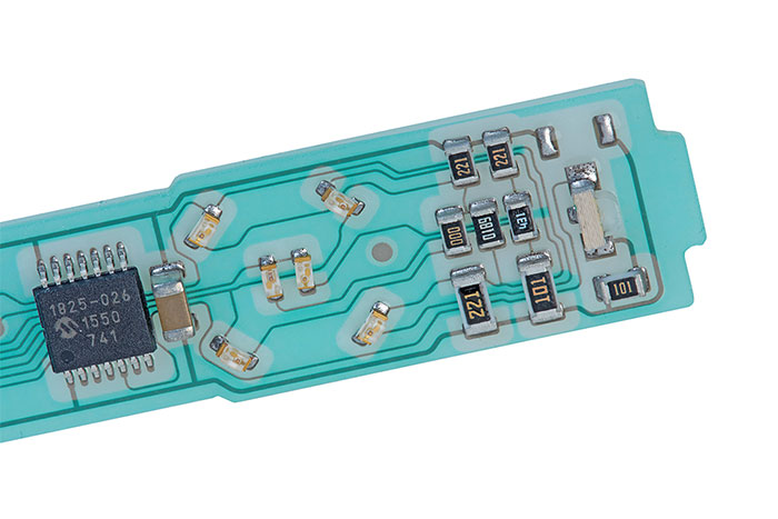
Figure 1. LEDs, resistors, capacitors and an integrated circuit bonded to a silver printed circuit via a low-temperature SMT process.
Cheaper films. When cost is a key design driver, silver circuits can offer a cost-effective, flexible solution. Polyester- based films are less than one quarter the cost of the polyimide sheets used in FPC copper circuits. This is especially true with oddly shaped circuits with poor material utilization. Additionally, silver circuits are made using far simpler manufacturing processes.
The first step to manufacturing an additive printed circuit is to choose the base substrate. Polyester (PET) is the most cost-effective and widely used base substrate, but not the only available option. Manufacturers print on polyimide, woven and non-woven fabrics and even paper, depending on the end-use application. Silver flake and carbon-based inks are the most common and widely available inks for printing conductive traces. New inks are constantly being developed (nano-particle inks a recent example), promising enhanced printing capabilities, higher conductivity or other desirable properties. Ink selection is application-specific and can depend on several factors, including the required trace resistance, trace width, curing condition or environmental and mechanical requirements (stretchable inks, scratch-resistant inks). The printing method will also come into play since the same ink will not be used for both flexographic and screen printing.
The printing process starts with either a sheet-fed or roll-to-roll printing process applying the conductive ink to the chosen substrate. Once applied, the ink must cure. Solvent-based inks cure in a matter of minutes using either a traditional conveyor-based or batch oven at 200° to 300°F. Most dielectric inks are cured via ultraviolet (UV) light. After the ink has cured, a dielectric print pass is applied where needed for electrical isolation or environmental protection. If multiple conductive trace layers are required, the process is repeated until the required circuit has been created. The process is highly efficient, produces little waste and does not require waste water treatment.
Similar to typical PCB assembly, a conductive bonding material (typically silver epoxy or solder) is then dispensed on the pads of the circuit. Standard pick-and-place equipment places surface mount components on the printed circuit. Standard SMD components, including QFN and QFP packages, may be used, but through-hole and BGA components are not currently suitable. Silver epoxy requires a constant temperature oven cure, while solder attach uses a traditional reflow oven and temperature profile. In the final step of the attachment process, a UV-encapsulant is dispensed onto the components, which, when cured, makes the circuit more resistant to vibration and mechanical shock.
Conversely, traditional rigid and flexible copper circuits are fabricated via a subtractive method. The process starts with a sheet of polyimide or FR dielectric bonded to a sheet of copper. The desired conductive paths are masked before a wet chemical process etches away all unwanted copper, leaving only the desired circuit patterns. In most cases, significantly more copper is removed than remains on the circuit, making for inefficient material usage. Adding more than two signal layers also requires additional press, drill and plating processes. A two-layer copper circuit has roughly twice as many processing steps as an equivalent silver printed circuit. Additionally, due to the many wet chemical processes, etched copper fabrication facilities are required to have waste water treatment and filtration systems, as well as highly monitored chemical storage areas.
Printed silver circuits open the door to greater product innovation in virtually any application, from high-end, sophisticated electronics to frangible, disposable, and other lower-cost devices. Relatively inexpensive polyester provides a flexible substrate alternative to a rigid PCB and a much more cost-effective alternative to copper FPC.
Screen-printed silver and roll-to-roll printed flexible circuits are proving to be a viable replacement technology for myriad applications, including:
- Low-cost disposable sensor products, including adhesive tags, RFID and data logging devices.
- Economic alternative to FPCs in portable and mobile devices, like wearables, personal diagnostic sensor devices, fitness equipment and fashionables.
- Tamperproof bottles and other frangible applications requiring a breakable circuit.
- Medical sensor equipment, like lightweight circuits for EKG leads and oxygen sensing.
- Home appliances and controls, including white goods, kitchen equipment and heating/air conditioning.
OEM design engineers should not overlook economical, high-performing silver flexible circuits with finely spaced silver traces and complex components on a polyester substrate. Depending on the application, printed silver circuits on polyester can save 25% or more on the substrate cost compared with an equivalent copper circuit. Engage with an experienced and qualified supplier early in the product design phase to maximize efficiencies and cost-benefits of screen-printed silver flexible circuitry.
Greg Kuchuris is marketing manager, printed circuit solutions, Molex (molex.com); This email address is being protected from spambots. You need JavaScript enabled to view it..


