Performing manufacturability checks early to reduce time to market.
One of the great challenges of bringing a new electronic product to market is validating the design against the requirements of the printed circuit board (PCB) manufacturing process. The challenge is acute for OEMs that use boards built by different contract manufacturers using different processes, because each may have their own particular design rules.
Each of the contract manufacturers typically changes the design to make it work for their process, and sends these changes back in the manufacturing format to the OEM. The OEM is then typically responsible for reconciling and validating changes from multiple manufacturers. This process often occupies considerable time in the late stages of the product development cycle, when changes are most expensive and a mistake can cause the product to miss the market window.
A new generation of design for manufacturing tools makes it possible to validate the design against design rules of all technologies and manufacturers that will be involved with the product in the early stages of the product development process. These design rules can easily be modified to accommodate additional processes or manufacturers or to address special conditions. Validating the design early substantially reduces and, in some cases, eliminates the need for late-stage design for manufacturing (DfM) changes, reducing engineering costs and making it possible to bring product to market earlier.
The DfM validation challenge has increased over the past decade, thanks to the proliferation of new and more popular manufacturing technologies, such as flex boards, rigid-flex hybrids, chip-on-board, embedded components, low-temperature co-fired ceramics, etc., each of which has its unique requirements. Each contract manufacturer generally has its own specifications for each of these technologies, creating a potentially large number of different design rule sets against which the design might have to be checked, depending on the technologies and manufacturers used. The nature of the PCB manufacturing process creates the potential for confusion and mistakes that are expensive and time-consuming to resolve late in the design process. For example, a leading cellphone OEM might use seven different flex board manufacturers, each of which uses different design rules and specs for different products and different lots of the same product. The design for a particular product either needs to be compatible with all the manufacturers involved in building the product. or different versions of the design must be used for different manufacturers.
Obtaining all the different design rule sets needed to perform DfM checks in and of itself can be a time-consuming process. Also, most PCB design software is not intended for the task of performing DfM checks. In such cases checks must be performed manually, which takes a considerable amount of time and is prone to errors. For instance, a flex circuit coverlay, sometimes called coverfilm, is sometimes used to encapsulate and protect the external circuitry of a flex board. Most PCB design tools consider coverlay and anything else outside the rigid board as dumb layers that are not included in design rule checks. However, coverlay layers can be important from a DfM standpoint in the common situation where holes are punched in the board. In a typical case, 5 mils clearance from each hole must be provided in the coverlay layer to avoid shorting with the mounting screw. Confronted with these difficulties, the majority of OEMs rely on the manufacturer to check the design after it has been completed.
One problem with this approach is the product developer is faced with the difficulty of validating the changes made by the PCB manufacturer or manufacturers to ensure they do not affect product functionality. In a typical example, different conductive materials require different line widths and spacing. If the PCB designer is not sure of the manufacturer, they may have a tendency to push out the spacing to avoid problems late in the design process. But increasing spacing from eight to 10 mils raises manufacturing cost.
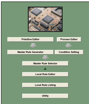
Automating the process. Next-generation DfM software addresses these challenges by providing a platform for storing design rules from a wide range of contract PCB manufacturers and processes, while interfacing with the PCB design software to automate the process of applying these rules to specific designs at any stage of development. A key aspect of these tools is the cooperation provided by PCB manufacturers in providing design rules for many of their processes and production equipment. This means product developers can simply select the manufacturer and process used for a particular board to perform a DfM rule check (FIGURE 1).


Figure 1. Web-based wizard to ease DfM rule creation.
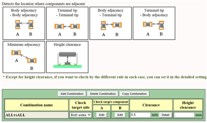
Of course, rules can also be entered manually when needed for manufacturers or processes that are not included in the database. The design rules are held in the cloud and updated in real time, so the information included is usually the latest that is available. The rule manager can handle more than 900 individual design checks that cover both bare board manufacturability and component mount checks (FIGURE 2).

FIGURE 2. Manage configurable layer view sets to support review of check results.
Web application. A web application running in a standard industry browser enables users to pick the rule decks to check the design against, modify rules on the fly as needed, browse violations, build a spreadsheet with a list of violations and sign off on the design. Unlimited combinations of design specifications, including place of production and production methods and materials, can be effectively managed. Rules are presented in an easy-to-understand format that does not demand computer-aided design (CAD) experience to interpret. Specifications, including manufacturing requirements, are shared in real time across design teams, locations and companies. Because data are held in a common, central database, updatable in real time, constraints are always based on the latest available information for the production machines in use. Rules are comprehensive and customizable, and the knowledge gained with each design is accumulated into a knowledge database to benefit future designs. The system facilitates accurate, efficient communications between PCB manufacturer and assembly plant, between OEMs and design bureaus, and between the OEM's headquarters and subsidiaries. Changes made to the design by the manufacturer are identified, and the manufacturer has the opportunity to enter reasons for these changes.
Typical DfM rule checks. For example, the area around a board clipping part is placed under considerable load when the board is divided. So it is important to consider interference and clearance of components from the board clipping part. This rule is often different from the typical component to board edge rule, so most PCB tools cannot differentiate and end up designing to the worst case, thus wasting real estate or making it necessary to manually resolve these issues late in the design process at a considerable cost.
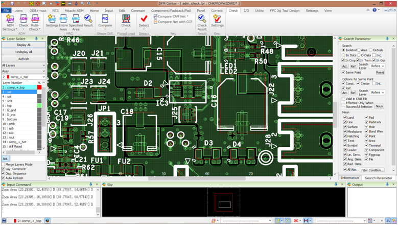
The DfM system will report errors if a part is placed closer than the ruled distance from a V-cut, router part, perforation or stressed part (FIGURE 3). It’s also important to look at pins that are spaced closely together to maintain a specified clearance between adjacent pins in order to avoid the formation of a solder bridge. The pin on the corner undergoes additional stress, so its exposed copper area must be smaller to ensure connectivity is maintained.

FIGURE 3. Checking component clearance from board clipping part.
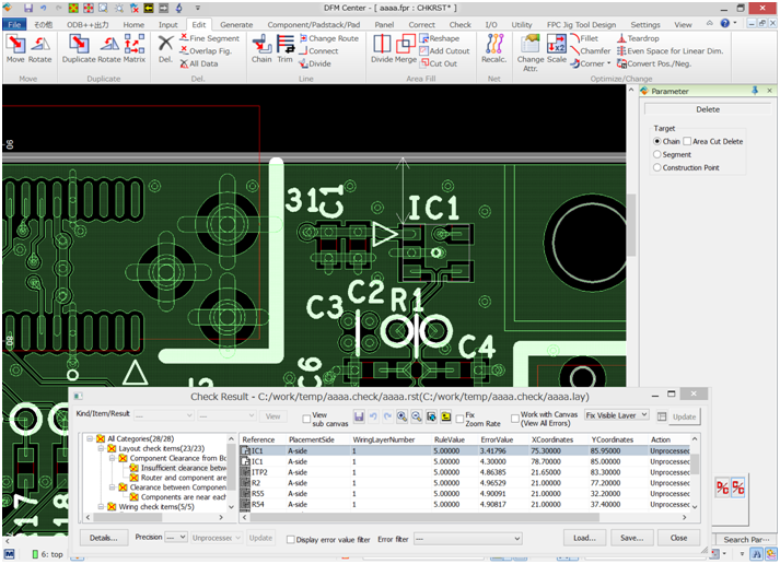
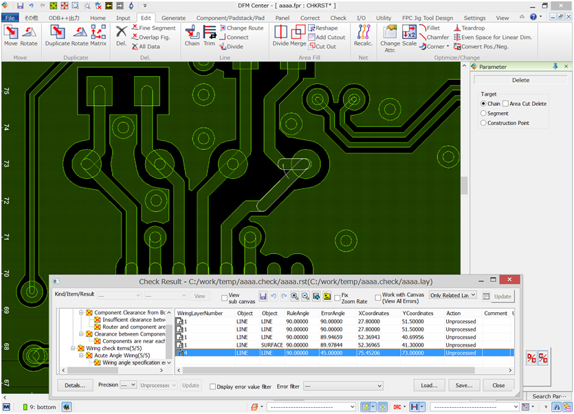
Another typical DfM check arises from the fact that if the wiring angle of a trace is too small, over-etching could cause an open circuit. This problem can be avoided by checking to be sure wiring angles are at or above a specified value (FIGURE 4). Finally, if the copper foil ratio differs by an excessive amount between two adjacent pins, the solder coagulation time of the pins will differ and may cause tombstoning, where one end of the chip component is detached from the copper pad of the PCB and stands on the other end of the chip component. The rule check measures the maximum copper foil ratio difference between the pins and issues a violation if it is greater than the specified value.

FIGURE 4. Wiring angle rule check.
In the design and production of electronic products, manufacturability checks are difficult to perform manually and are often made after the design process is complete. However, this approach is rapidly becoming untenable due to increasing design complexity, greater global design collaboration and tighter product delivery schedules. The new automated approach to DfM efficiently manages the growing number of design rule checks needed to ensure manufacturability early in the design process and concurrently as the work progresses, ensuring designs have been produced in accordance with component mounting and manufacturing specifications. The entire process is front-end driven, sharing data in real-time across all departments, divisions, and companies involved in the design and development of an electronic product. This approach reduces design iterations because rule checks are run as design work progresses, and problems are identified early in the design cycle. Design time and costs are reduced through faster design reviews, fully documented checks and the ability to set up checks and rules specific to the manufacturing processes and equipment used. Products are manufactured right the first time, reducing time-to-market and time-to-volume.
Humair Mandavia is the Chief Strategy Officer at Zuken (zuken.com); This email address is being protected from spambots. You need JavaScript enabled to view it..


