Overcoming problems of nominal dimensions of the trace and board to calculate resistance.
Designers and engineers are sometimes concerned about the voltage drop across a trace. With today’s low impedance circuits, such voltage drops may introduce an unacceptable amount of noise or signal level uncertainty into a circuit. These engineers are also concerned about the potential voltage drop across a via. Some are so concerned that they try to avoid the use of vias on boards altogether. In this article, we will show how to predict the voltage drop across a trace, and show that the voltage drop across a via is almost negligible by comparison.
The voltage drop across a trace or via is a relatively simple calculation using Ohm’s Law, V = I*R. But there are some hidden complexities in this relationship when it comes to determining R, the resistance of the trace:
1. R depends on the resistivity of the conductor, which can vary by as much as 5%, depending on whether the copper used for the trace is rolled, electrodeposited, or a combination of the two (as in the top layer of a fabricated board).
2. R depends on the temperature of the trace. The thermal coefficient of resistivity of copper ranges from 0.0038 (1/°C) to 0.0040 (1/°C), depending on the reference (another 5% variation). So the trace temperature must be known and considered.
3. R depends on the thickness of the trace. The IPC specification on trace foil thickness is 10%. If the trace is copper-plated by a fabricator, the thickness can vary around the board by as much as 50%, and this thickness can even be variable along the length of the trace.
These uncertainties point out the problems in using the nominal dimensions of the trace and board to calculate the resistance. On the other hand, the resistances are typically so low that accurately measuring them is not easy (assuming the board is already designed and fabricated).
The basic formula for the resistance of a trace is given by Equation 1:
R = ρ * L / A [Eq. 1]
where: R = resistance
ρ = resistivity of the copper material
L = length of the trace
A = cross-sectional area of the trace, W * Th
where: W = trace width
Th = trace thickness
The resistivity of the copper material, and therefore the resistance, is a function of temperature. So if resistivity is specified, it is always specified at a specific reference temperature, typically 20°C. Then the resistivity at any other temperature is given by the relationship in Equation 2:
ρ(T) = ρ(To)*(1+αo*(T - To)) [Eq. 2]
where: T = temperature of interest
To = reference temperature
ρ(T) = Resistivity at the temperature of interest
ρ(To) = Resistivity at the reference temperature
αo = Thermal coefficient of resistivity at the
reference temperature.
If we know the resistance of the trace at any temperature, and we wish to know the resistance at any other temperature, simply substitute R for ρ in Equation 2 (Equation 3):
R(T) = R(To)*(1+αo*(T - To)) [Eq. 3]
where: T = temperature of interest
To = reference temperature
R(T) = Resistance at the temperature of interest
R(To) = Resistance at the reference temperature
αo = Thermal coefficient of resistivity at the reference temperature.
Examples
We will provide the calculations for two sample traces, each one for a simple straight trace and for a trace with a via in the center. In the next section we will show the results of a simulation for each trace to see if the results of the simulation square with the calculations.
The sample traces will have the following characteristics:
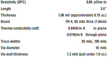
The via and trace dimensions have been specifically selected so the 26 mil wide trace and the via have approximately the same cross-sectional areas (convenient for use in Equation 1).
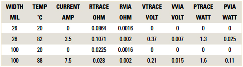
The resistance at 20oC for the 26 mil trace is found from Equation 1:
R20 = 0.68*3.5 / (26*1.06) = 0.0864Ω [Eq. 4]
The designer or engineer can now use Ohm’s Law to calculate the voltage across this trace at any level of current and determine if that level of voltage might cause a problem.
For higher levels of current, the temperature rise associated with that current needs to be taken into consideration. For example, let’s apply 3.5A current through this trace. We have determined through modeling1 and various calculators that this will raise the temperature of the trace to about 83oC. The resistance at 83oC is found from Equation 3:
R(83°) = .0864*(1+.0038*(83 - 20)) = 0.1071Ω [Eq. 5]
At 3.5A, the voltage drop across this trace is:
V(83°) = 3.5 * 0.1071 = 0.37V [Eq. 6]
For comparison, the voltage drop across the trace at 20°C would have been:
V(20°) = 3.5 * 0.0864 = 0.30V [Eq. 7]
Although this might be a significant voltage drop, this example was specifically constructed to be a “worst-case” situation, as 83° is a higher temperature than most designers will allow.
The same resistance calculations for a 100 mil wide trace get the following:
R20 = 0.68*3.5 / (100*1.06) = 0.0225Ω [Eq. 8]
The wider trace results in a much lower resistance. This is, of course, one obvious way to reduce the trace resistance and therefore the voltage across the trace. A current of 7.5A will raise the temperature of this trace to a similar temperature as above, this time 88°C. Thus, the resistance and voltage across the trace at temperature is found by:
R(88) = 0.0225*(1+0.0038*(88 - 20)) = 0.028Ω [Eq. 9]
V(88) = 7.5 * 0.028 = 0.21V [Eq. 10]
Although a much higher current is applied across this wider trace, the resistance and voltage drop are much lower because of the increased width.
Effect of via. The 10 mil diameter via has approximately the same cross-sectional area as a 1.0 oz., 26 mil wide trace. Thus, the via can be represented as a 63 mil long, 26 mil wide trace. We can approximate its resistance and temperature several ways:
1. Plug its dimensions into Equation 1 and calculate its resistance directly.
2. Simply look at the ratio of the length of the via to the length of the 26 mil trace whose resistance is already known.
Using this second approach, via resistance at 20°C can be estimated as:
Rvia = 0.0864 * (0.063/3.5) = 0.0016Ω [Eq. 11]
That is, the resistance of the via is, in this case, only 1.8% of that of the 26 mil trace and 7.1% of the 100 mil wide trace! Considering the other uncertainties involved, this is almost trivial.
We have shown in a previous article2 the temperature of a via is determined not by the current through the via but by the temperature of the trace. Therefore, only a single small via is needed regardless of trace size. Since these relationships are linear, we can approximate the resistance of the via at the higher temperatures as:
For 26 mil trace: Rvia at 83° = 0.1071*0.018 = 0.002Ω
For 100 mil trace: Rvia at 88° = 0.028* 0.071 = 0.002Ω
It is expected these last calculations are equal because they relate to the same via raised to almost the same temperature!
Even at the high currents used here, the voltage drops across the vias are still pretty small:
For the 26 mil trace: Vvia = .002*3.5 = 7.0 mV
For the 100 mil trace: Vvia = .002*7.5 = 15.0 mV
TABLE 1 summarizes these results.
Table 1. Summary of the Calculations
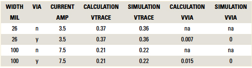
Simulations: As in previous studies,3 we can use the TRM (Thermal Risk Management) simulation tool to simulate these traces. One of the many outputs of a TRM simulation is a voltage profile. This allows us to determine the voltage at any point along a trace or via. We use TRM to simulate these two traces, with and without vias, at the currents specified, except we can’t simulate zero current! TABLE 2 compares simulation results with the results calculated above. The simulation compares almost exactly with the calculations.
Table 2. Comparison of Calculated and Simulated Results
Conclusion
The voltage drop across a trace may or may not be significant enough to affect the system operation. The system design engineer has the responsibility to determine this. But it is likely the voltage drop across a via is trivial, even at higher temperatures, especially compared to the voltage drop across the parent trace.
Notes
1. See, for example, Douglas G. Brooks, Ph.D. and Dr. Johannes Adam, “Trace Current/Temperature Relationships,” PCD&F, June 2015. See also Brooks and Adam, “PCB Trace and Via Currents and Temperatures: The Complete Analysis,” available at amazon.com.
2. Douglas G. Brooks, Ph.D. and Dr. Johannes Adam, “How Hot Is My Via? (Cooler Than You Think!),” PCD&F, October 2015.
3. For example, see references in Notes 1 and 2.
Douglas Brooks, Ph.D., is president of UltraCAD Design, a PCB design service bureau and author of PCB Currents: How They Flow, How They React; This email address is being protected from spambots. You need JavaScript enabled to view it.. Johannes Adam, Ph.D., CID, is president of Adam Research, creator of Thermal Risk Management software, and a member of the IPC 1-10b Current Carrying Capacity task group.


