The second of a series on DDR considers how to speed up the process of designing a functioning system.
In the previous article,1 we discussed some critical signal integrity concerns engineers face while designing the DDR bus. Given these challenges, it is usually wise to simulate the design before fabricating the board. Doing so will greatly increase the odds of a functional board on the first pass, and will reduce the number of spins required for the design. That said, the time required to set up, run and analyze the simulation also needs to be fast enough to make the investment in simulation worthwhile.
So, the goal of the design engineer is to use a tool that permits a quick simulation setup, runs the simulation in a reasonable amount of time, and provides data that are easy to understand and parse so the critical data can be focused on. The ideal tool needs to do all this while also providing data accurate enough to be useful.
To shorten setup time, it’s often beneficial to be familiar with the required data and have them ready by the time of the simulation. There are really only a handful of items needed for a successful run. Most of these items are either already available to the designer, such as a board file, or available through vendors of the different parts. The required items can be thought of as a checklist.
The first items required are the driver and receiver models for the memory controller and DRAMs. The controller’s IBIS model can usually be accessed by contacting the controller vendor’s AE, or can often be accessed on the manufacturer’s website. Similarly, the DRAM IBIS models can be accessed from DRAM vendors such as Micron, Samsung or Hynix. The models should contain information for the different driver strength options, as well as the different ODT termination options available to the respective chips.
Some vendors opt to provide Spice models, rather than IBIS models. While Spice simulations can be marginally more accurate, they are often orders of magnitude slower to execute. A presentation last year2 highlights a simulation setup that took 221 hours to run the Spice driver version and only three hours to run the IBIS driver version, with only a marginal hit to accuracy. So, if time is a concern, using an IBIS model could speed up the process. That said, there have been cases of poorly created IBIS models, so it might benefit the design engineer to request correlation data from the vendor.
The next requirement is the pass/fail criteria for the different ICs. While simulation tools can generate waveforms, only the chip vendor can provide the measurement criteria to categorize the resulting waveforms as acceptable or not. A simple example is the eye opening width required at the controller during read transactions on the DQ signals. These values are defined by Jedec for the DRAM memories, and are readily available either on the DRAM datasheets or from the Jedec website (jedec.org). The controller requirements can usually be obtained from the datasheet of the controller.
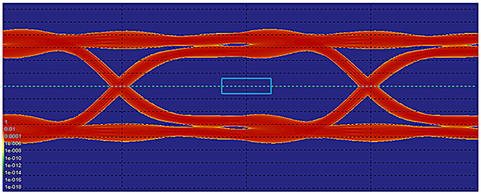
There are times, however, the controller vendor might not publish the requirements in its datasheet. In such cases, the best option might be to talk with the vendor’s applications engineer. Keep in mind these requirements are not simulation-specific, but are needed for characterization of your bus once the board comes back. After all, if there is an eye diagram on the oscilloscope, as shown in FIGURE 1, and no eye mask to go with it, then there’s no way of knowing how much margin the design has in volume production. So, in the discussion with the vendor’s AE, it might be better to focus on system SI validation rather than on simulation validation.

Figure 1. An eye diagram plots a large number of signal transitions on top of an eye mask (center rectangle) to reveal the operating margins. In this example, the operating margins are very good.
The common requirements to request from the controller vendor are:
- The input timing relation requirement between DQ/DQS during read transactions.
- The output DQ/DQS variations during write transactions.
- The output DQS/CLK variations during write transactions.
- The output address/CLK variation during address/command transactions.
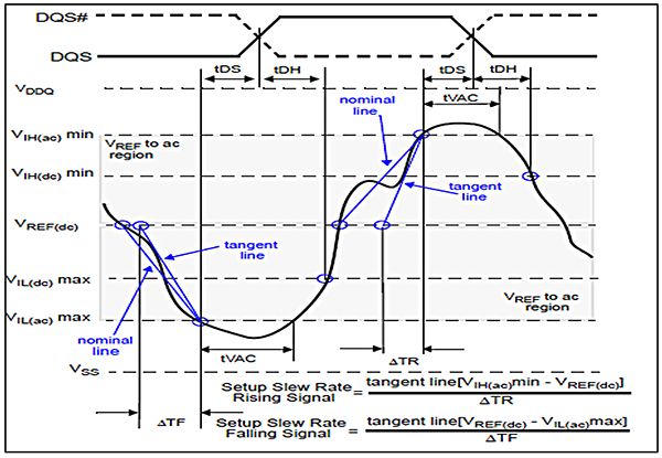
While the data for the controller might require some work to get from the vendor, information for DRAMs is available on the Jedec website. Note: The specification documents contain not just signal integrity-related information, but a whole host of data that might not be pertinent to validating the robustness of the DDR channel. While going through the specs, make sure to focus on the electrical section (FIGURE 2).

Figure 2. Jedec specs contain all the information needed for simulation.
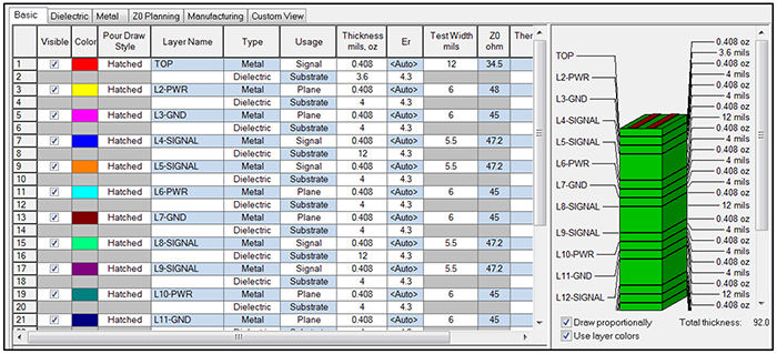
Next, the board stackup information needs to be accurate (FIGURE 3). These data are obtainable from the PCB vendor. The information here includes the layer assignments, trace widths (for given impedances) and dielectric properties. A tentative stackup should be available from the PCB vendor, even before fabricating the board, and can be used in the exploratory stage of design, before layout begins.

Figure 3. Stackups define all the layers in the board, including trace widths and dielectric properties.
Moving on, parts of the system where third-party models are required need to be identified. Connectors, for example, are best modeled by connector vendors. Connectors might be modeled as simple RLC networks or as a more detailed S-parameter model. It’s best to contact the vendor for these models. Similarly, if standard DIMMs are used in the system, the board models for the appropriate DIMM need to be used. The board models for the DIMMs can be obtained from Jedec too.
Finally, regions of the board that might need special analysis need to be identified. There might be structures in the designs best modeled using 3D solvers. Most often, these are vias without good return-path stitching. The higher the data rate, the more likely a via needs to be modeled as a 3D structure.
In summary, simulation needs to be used as a tool to speed up the process of designing a functioning system. Simulation should not in itself become a time hindrance for the project at hand. To ensure this, adequately preparing for simulation runs will go a long way toward reducing time required for simulating. This will require a bit of time analyzing the board, and a few emails to the DRAM, controller and connector vendors to get the models and timing requirement information. With this information in hand, you should be well on your way to validating your design, which we will look at in part 3.
References
1. Nitin Bhagwath, “Designing PCBs for DDR Busses,” PCD&F/CIRCUITS ASSEMBLY, June 2016.
2. Nitin Bhagwath, “DDR4 Board Design and SI Challenges,” DesignCon, January 2015.
Nitin Bhagwath is technical marketing engineer at Mentor Graphics (mentor.com); This email address is being protected from spambots. You need JavaScript enabled to view it..


