What determines the temperature of a via? Hint: It’s not the current.
In work published in October 2015, Johannes Adam and I estimated the internal temperature of a via using simulation techniques.1 What we concluded defied all conventional wisdom. It turns out the temperature of a via does not depend on the level of current through it. The via temperature depends on the temperature of the trace(s) it is connected to. This is because the thermal conductivity between via and trace is so good that any excess heat is conducted away from the via to the trace(s). Thus, a large trace carrying a large current needs only a single small via for connection to another similar trace.
If there ever was a conclusion that cried out “show me!” this is it! This month, we report on an empirical investigation that confirms the prior simulation.
The Test Board
The relevant portion of the test board is shown in FIGURE 1. The board is approximately 60-mils thick FR-4. The board contains 0.5 oz. copper nominally plated with 1.0 oz. additional copper. Two traces were compared, one nominally 27 mils wide, the other 200 mils wide. Each trace is 6.0" in length, one-half on the top layer and one-half on the bottom layer. Each trace has a single 10 mil diameter plated via connecting top to bottom. It is important to note the via structure is identical in each trace. The board was supported 2.5" above a plywood surface in still air by four screws at the corners. The board was microsectioned after testing to measure the actual dimensions for the simulation.2
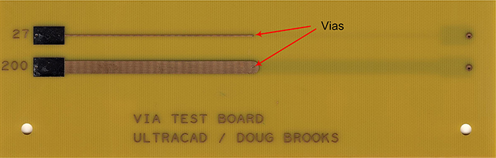
Figure 1. Relevant portion of via test board.
The 10 mil diameter via plated to 1.0 oz. has roughly the same conducting cross-sectional area as the 27 mil trace. That is why the 27 mil wide trace was chosen for this study.
The Simulation
It is difficult to simulate a via test on a board this size. The reason is the small via wall thickness. Think of the board as a three-dimensional object. We will model it in 3D using a wire grid made of many small cubes. Each individual cube is considered homogeneous. Therefore, the set of equations solves for the boundary conditions associated with each cube. The dimension of the cube must be smaller than the smallest dimension modeled (the via wall). The smaller the cube, the more cubes in a given volume. The sizes of the calculational matrices are determined by the number of cubes. The load on the computer CPU is determined by the size of the matrices. To model the portion of the board shown in Figure 1 places a very large burden on even a moderately powerful modern desktop computer.
Therefore, for practical purposes we need to “trim” the model. We do this primarily by trimming two dimensions in the simulation (note: trace width and board thickness are not changed in the model):
- Shorten the overall trace to 3.5" from 6.0".
- Reduce the overall width of the board material.
The practical impact of these modifications is to reduce the cooling of the trace being simulated. Therefore, we expect a result that is slightly higher (hotter) than actual, particularly at higher currents.
An important parameter in any thermal model is the thermal conductivity coefficient for the dielectric. Rather than trust estimates on the Web and the sometimes incomplete measures found on datasheets, a sample of board material was sent to C-Therm in Canada. It measured the thermal conductivities as (W/mK):
- In-plane 0.679
- Through-plane 0.512
Simulation Results
TABLE 1 shows the results of the simulation. They are consistent with the results presented in Brooks and Adam in October 2015.1 For a small trace, approximately the same size as the via, the via is cooler than the trace because the via cools more effectively into the dielectric layer of the board than does the trace. For the larger trace carrying more current, heat generated in the via is conducted away from the via onto the trace, resulting in the via being a little hotter than the trace (but not a lot).
Table 1. Via Temperature Simulation Results
FIGURES 2 and 3 are the simulated thermal profiles of the 200 mil trace carrying 8.55A and the 27 mil trace carrying 6.65A, respectively. Note the thermal profile cools a little near the via for the 27 mil trace. The via is the hottest point on the 200 mil trace, but only 7.4% hotter than the trace itself.
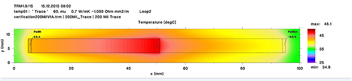
Figure 2. Thermal profile of 200 mil trace carrying 8.55A.
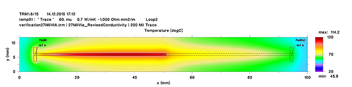
Figure 3. Thermal profile of 27 mil trace carrying 6.65A.
Test Procedure
The test equipment list included the following: constant current generator, Dr. Meter DC Power Supply HY3010E; temperature measurements, Omega Instruments data logger model OM-EL-USB-TC-LCD with type K probe; Pico Technologies portable oscilloscope model 2204A; TekPower model TP9605BT digital meter (to check current levels).
The test procedure is fairly straightforward. A constant current is applied to the trace. The current level is checked and confirmed by a second digital meter. Temperature is measured with a thermocouple probe whose tip diameter is specified at 30 Ga. (approximately 10 mil diameter). The probe response time is approximately 1 sec. The probe was calibrated to an ice cube and to boiling water at an elevation of 360' and found to be perfectly calibrated. Various tests were run to verify the probe does not affect the temperature of a trace being measured.
For each test, a constant current is applied to the trace until the temperature stabilizes (approximately 6 min.). Then the temperature is measured and recorded. After the measurements were taken, the board was returned to Prototron Circuits for microsectioning to confirm all dimensions.
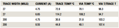
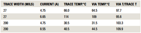
Measured Test Results
The measured test results are provided in TABLE 2. Two especially important observations should be made:
- First, a 6.6A current through the 27 mil wide trace results in a via temperature of 109°C, while a higher current of 8.6A results in a larger (200 mil wide) board results in a much lower via temperature of only 44.5°C. This confirms the trace is controlling the via temperature.
- The simulation data are very close to the measured data. This gives us confidence the simulation approach is a viable approach for predicting temperatures in complex situations.
Table 2. Measured Results of Via Tests
Conclusion
The results of this evaluation are consistent with, and seem to confirm, the results reported in our earlier paper. It is not the current that determines the temperature of a via; it is the temperature of the associated traces. If the traces are sized correctly for the current level, much smaller and fewer vias are required to transition between trace layers than has been previously believed. This means designers can have much greater flexibility in freeing routing channels underneath the traces on their boards.
References
1. Douglas G. Brooks and Johannes Adam, “How Hot Is My Via?” PCD&F, October 2015, vol. 32, no. 10.
2. The trace widths were essentially as designed. The thicknesses were (top layer) 2.1 mil and (bottom layer) 2.9 mil.
Acknowledgments
This type of study would not have been possible without the cooperation of several people and organizations. In particular, I want to thank my longtime partner Dave Graves (now with Monsoon Solutions in Bellevue, WA) for helping prepare the final artwork for the test board. C-Therm Technologies (Fredericton, New Brunswick) graciously measured the thermal conductivity of the board material to facilitate the simulation. And a special thanks to Prototron Circuits, Inc. (Redmond, WA), which provided the test boards and also the microsectioning work and measurements. And my collaborator on trace thermal issues, Johannes Adam (Leimen, Germany), continues to be a great help in evaluating results.
Douglas Brooks, Ph.D., is owner of UltraCAD Design, a PCB design service bureau and author of PCB Currents: How They Flow, How They React; This email address is being protected from spambots. You need JavaScript enabled to view it..


