Why smoothing copper for better signal integrity could degrade mechanical performance.
Most every electrical engineer working with high-speed differential interfaces such as PCIe is aware of the effect of rough copper on insertion loss – and knows it is to be avoided. What they may not understand is exactly why that’s true. There is a common explanation that seems intuitively correct but isn’t, that the current follows the longer contour of the copper, and the longer travel distance is responsible for the increased loss when using rough copper. To understand what’s actually happening, we have to move from a “circuit” model of signal propagation to a “fields” model.
Modern high-frequency signals are at microwave frequencies, forcing even digital designers to understand different fundamental physics than we’re familiar with.
We are used to a “circuit” model of signaling, where current leaves the signal pin of the transmitter and returns via the ground pin of that transmitter, making a loop through the PCB and receiver, completing the circuit. In the “fields” model that we have to get comfortable with at higher frequencies, however, the transmitter sets up electric fields between the signal and ground pins, and the energy in those fields is guided by the package, PCB, and connector features (such as pins, traces, and vias) to the receiver. The “fields” model better explains the effects of vias, return path transitions, and attenuation of the signals due to dielectric and copper losses. Why does rough copper absorb more energy than smooth copper? In short, it isn’t because the “current” travels farther (as in the “circuit” model); it’s because the electromagnetic energy is exposed to more copper surface.
A “circuit” model explanation of why rough copper absorbs more energy than smooth copper as a signal propagates from transmitter to receiver focuses on the “current” traveling a longer path due to the rough copper. For instance, in FIGURE 1, it’s intuitively clear the current travels a shorter distance on the surface of smooth copper than rough copper; thus it loses less energy (assuming the notion of “skin depth” forcing “current to flow on the surface of conductors” has been explained elsewhere).
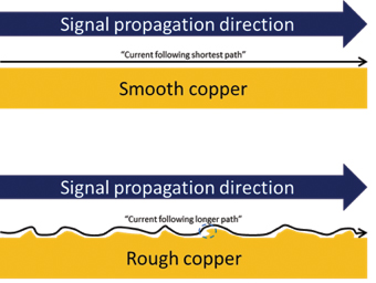
Figure 1. “Current” on smooth and rough copper.
There are some problems with this intuitive explanation, however. If it were accurate, the signal would be delayed in rough copper proportionally to its lost energy.
Measuring the propagation delay of signals on rough and smooth copper doesn’t support that; their propagation delays are very similar. Also, note in the area circled that the rough copper may not be continuous from left to right. What happens here? Does the current loop back? We have to use the “fields” model to better understand what is really happening.
In the “fields” model, the signal propagates from left to right as an electromagnetic wave in the dielectric, inducing current density waves in conductors subjected to those waves (both signal and “ground,” or any other adjacent conductor). For instance, in FIGURE 2, we have a simple step source generating a fast rising edge voltage on a signal trace (*A). At the instant it’s applied to the trace, that changing voltage generates a positive-going charge on the “signal” (*B) and a changing electric field (“e-field”) between the signal and “ground” (*C).
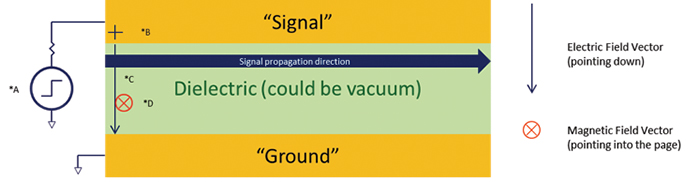
Figure 2. Signal propagating from source.
The changing e-field induces a changing magnetic field (“h-field,” *D) into the page, since the signal propagates from left to right. That changing horizontal (tangential) h-field induces an e-field to the right, and this continues as an e-field/h-field leap-frog, as long as the signal and “ground” are well-behaved, allowing the signal to propagate through the dielectric, guided by the signal and ground structures. The wave propagation is in the direction of the cross product of the electric and magnetic fields. Using the “right hand rule,” with the index finger of the right hand pointing in the direction of the electric field (down) and the middle finger pointing in the direction of the magnetic field (into the paper), your thumb will point in the direction of propagation (to the right). This use of the right hand rule is called the Poynting vector.
As the signal propagates in the dielectric, electric charge density changes on the surface of the conductors (both signal and “ground”). Those waves of current charge density follow the signal, making it appear there is a current flowing from left to right in the conductor, and right to left in the “ground.” This is how it appears in the “fields” model. This model might seem awkward to comprehend at first, but it has a distinct advantage in explaining the effect of copper roughness. Rather than thinking of current flowing on the surface of the conductors, we can instead think about the effect of the electromagnetic field on those surfaces.
If we focus on the dielectric/conductor interface (FIGURE 3), fundamental electromagnetics forces very different behaviors within the dielectric and conductor. Inside the dielectric, on the surface of the conductor, the e-fields must be perpendicular to the conductor surface (perfectly so for a perfect conductor, or PEC, nearly so for a “good conductor”). Inside a good conductor, the changing e-field can’t continue in the vertical direction. The changing h-field, however, is continuous across the boundary of the dielectric and conductor. In other words, at the exact surface of signal (and ground), the changing magnetic field intensity is the same in the conductor and dielectric. Inside the conductor (assuming it isn’t a perfect conductor), that changing h-field induces changing e-fields and associated eddy currents, and energy is absorbed. The intensity of the magnetic (and electric) fields drops exponentially as the energy propagates up into the conductor (as shown by the reduction in opaqueness in Figure 3), dependent on the frequency of the changing fields. We refer to the distance it takes to reduce their intensity down to 1/e as the “skin depth.” Note that this energy in the conductor propagates orthogonally to the dielectric signal propagation (vertical vs. horizontal, respectively, in these illustrations), and is much slower, at a rate thousands of times slower than in the dielectric.1 The magnetic field will be in the same direction (into the page) as in the dielectric, but the electric field will be left to right, and the energy propagation is from bottom to top. An analogy to the propagation of energy in the conductor due to that in the dielectric is the wake of a speedboat – it travels perpendicular to the boat’s direction of travel.
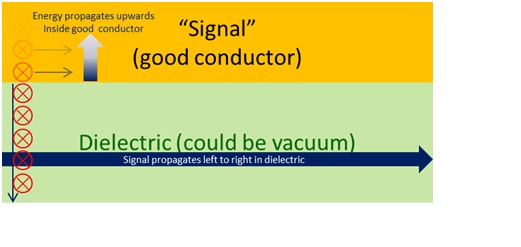
FIGURE 3. The dielectric/conductor interface.
If the frequency is low, the induced eddy currents are small; not much energy is lost as the wave propagates, and that wave might extend through the entire thickness of the conductor. This is the case where the “skin depth” is greater than the conductor thickness. As the frequency increases, the skin depth becomes very small. At microwave frequencies the copper roughness is often greater than the skin depth. For instance, at 5GHz, the skin depth for copper is approximately 1µm,2 while standard 1oz. copper can have a roughness profile of 3µm.3 In the “circuit” model we would say the vast majority of the current is traveling on the rough surface. In our new “fields” model we picture the electromagnetic energy propagating slowly into the conductor, but only traveling a very short distance inside that conductor (1µm) before being absorbed by the conductor as eddy currents and heat.
FIGURE 4 demonstrates the two different models representing the same signal propagating from left to right, and its effect on a rough signal trace (conductor). We have replaced the circuit model of current traveling a longer distance on rough copper with a fields model of the electromagnetic energy impinging on a larger surface area as it propagates from left to right adjacent to a rough conductor. The fields model gives us some intuition that the increase in loss due to copper roughness is going to be proportional to the increased conductor area that the fields are subjected to. Unfortunately for us, the peel strength of the copper is also going to be proportional to that same area. Any effort to smooth the copper for better signal integrity will degrade the mechanical performance. Laminate suppliers will have to use chemical bonding means to retain peel strength (mechanical strength) while smoothing the copper for better signal integrity.

FIGURE 4. Circuit vs. fields model of trace.
As a side note, the fields model can also be used to better understand the purpose of the conductive wrapper in “Hot Pockets” and other microwavable foods (some chicken pot pies, for instance). The wrapper quickly absorbs the microwave energy and heats the outer surface of the dough, browning it. They also may make use of the Curie temperature (then point at which some materials’ magnetic properties change dramatically) to limit the effect, but I’m not able to confirm that. Explaining the same effect using a circuit model would be extremely difficult.
The point is not to replace the circuit model of signal propagation with a fields model for every frequency, application, or problem. Rather, it is to augment the
circuit model with another that sometimes is more useful to understand the fundamental physics behind an issue. There are other cases where a fields model can enhance the intuition behind a problem (crosstalk and via impedance, for instance); it’s a good idea to understand it at microwave frequencies.
Ed.: This version contains text and illustrations not included in the original print version.
References
1. Paul G. Huray, Maxwell’s Equations, John Wiley & Sons, 2010, p. 231.
2. Dr. Eric Bogatin, Signal Integrity – Simplified, Pearson Education, 2010, p. 192.
3. Rogers Corp. white paper, “Copper Foils for High Frequency Materials,” 2015, Table 1.
Jeff Loyer is signal and power integrity product manager at Altium (altium.com); This email address is being protected from spambots. You need JavaScript enabled to view it.. He spent more than 20 years as an engineer at Intel, the past 10 as signal integrity lead.


