Simulations demonstrate vias can carry substantially more current than assumed.
Most people don’t have any idea how hot a via gets. After all, it’s hard to get a temperature probe down inside the via to find out, at least not without disrupting a lot of things. As far as we know, there haven’t been any studies of via temperature, and even the theoretical approaches that exist are pretty approximate. So we set out to answer that question through simulation.
In two previous papers1 the authors explored the current/temperature relationships of PCB traces under normal current loads and under a significant overload of what would be considered the normal current carrying capacity of the trace (“fusing” current and time.) But through the years there has been very little written about the current carrying capacity of a via.
A via typically has a drill diameter and a copper conducting thickness formed during a plating process. This gives the via a conducting cross-sectional area.2 There are fabrication limitations on the minimum size of a via drill diameter, and tolerances on plating thickness. But the bottom line is, how big does the conducting cross-sectional area need to be to handle the current?
Board designers typically approach this question using one of three strategies:
- Don’t permit vias that carry higher levels of current. Route all the conductors on the same trace layer.
- Size the via to handle the current using IPC-2152, “Standard for Determining Current Carrying Capacity in Printed Board Design,”3 guidelines.
- Use a “standard” via known to be able to carry a certain amount of current and use multiple vias in parallel, as many as needed for the total current carried by the trace.
IPC-2152 explicitly endorses the latter strategies3:
The cross-sectional area of a via should have at least the same cross-sectional area as the conductor or be larger than the conductor coming into it. If the via has less cross-sectional area than the conductor, then multiple vias can be used to maintain the same cross-sectional area as the conductor.
Anecdotally this must be good advice because most designers have never had a via fail for purely thermal reasons (unless there was a fabrication or alignment issue). What we’ve been doing must be right, because it works so well! In fact, we will show that this guidance has been extremely conservative.
But there is an implicit assumption in this guidance that sometimes poses a problem. That is, it is assumed we know the plating thickness of the via. We typically assume (hope might be a better word) that the via wall thickness is the same as the plating thickness, which is typically 0.5 or 1.0 oz. copper (0.65 to 1.3 mils). But the plating is often not uniform on the walls of the via. (This is a separate problem not addressed in this article.)
The authors have run thermal simulations on traces in the two referenced articles using a thermal simulation program called TRM (Thermal Risk Management).4 The techniques for simulating trace temperatures using TRM are explained in those articles. These same techniques can be applied to simulating the temperature of a via. In this article we will report the findings of a set of simulations on via currents and temperatures for a variety of trace sizes. The simulation tool allows us to “measure” the temperature at the midpoint of the via, as well as any selected point(s) on the trace itself.
We proceed with the following set of assumptions and strategies:
- We will assume a standard via with a 0.26mm (10 mil) drill diameter and a 0.030mm uniform plating thickness. This is slightly less than a 1.0oz equivalent. The effective cross-sectional area of this via is π(r2 – (r-th)2), where r is the via radius and th is the plating thickness. Choosing these mm values results in a via cross-sectional area of 0.0217mm2. This is approximately equivalent to a 1oz., 26 mil (0.66mm) wide trace.5
- The pad area of a via doesn’t matter because the traces are at least 26 mils (0.66mm) wide. (If the traces were smaller, the via cross-sectional area would exceed that of the trace and should be okay from a heating standpoint “by definition.”)
- We will be dealing with a standard board thickness of 63 mils (1.6mm). Additional simulations we have run do not suggest that increasing the board thickness has any significant impact on the results.
- We will vary the trace width and current and compare the temperature of the trace on the board with the via temperature. In this way, we will see if the via gets hotter than the trace, stays the same temperature as the trace, or runs cooler than the trace.
- We assume that at low currents via temperature is not a problem. Since we are primarily concerned with high-temperature effects, we will concentrate on what happens at higher temperatures and currents.
The first simulation we ran was for a 1.0oz., 0.66mm (26 mil) wide trace with a single via with diameter 0.26mm (10 mil) and wall thickness
0.03mm. The via cross-sectional conducting area was the same as that of the trace. Under the normal guidelines, we would expect the via temperature to be the same as the trace temperature (without a via). In fact, the via ran cooler than the trace! The results are shown in TABLE 1.
Table 1. Temperature (˚C) Simulation of 0.66mm Wide Trace
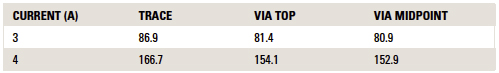
So how can the via temperature be less than that of the trace? One of the surprises of IPC-2152 is that internal traces are cooler than external traces of the same size carrying the same current. That is because the dielectric material of the board is a better conductor of heat than is convection or radiation into the air. The via looks more like an internal conductor than an external one, conducting more heat into the dielectric before it is shed by convection and radiation into the air. Therefore, it runs a little cooler. In fact, looking at Table 1, the via is coolest at its midpoint, and still cooler than the trace at the top of the via. The surprising result is that the via is helping cool the trace!
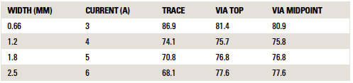
When we increase the size of the trace, and also increase the current, the situation changes a little. We ran simulations for trace widths of 1.2mm (47 mils), 1.8mm (71 mils) and 2.5mm (98 mils). But in every case the via dimensions were unchanged from before (TABLE 2).
Table 2. Temperatures in the Simulation at Various Points and Currents
All these results are plotted in FIGURE 1. In the figure, the trace sizes go from 0.66mm on the left to 2.5mm on the right. The black line is the trace temperature, and the red is the via midpoint temperature. It is assumed the trace temperatures go through the origin (0.0A) at 20˚C.
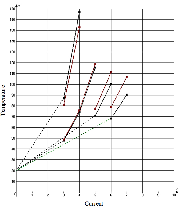
Figure 1. Via and trace temperature vs. current for simulated widths.
We have already discussed the fact that the via for the 0.66mm trace is cooler than (below in the graph of) the trace. When we increase the width to 1.2mm (and increase the current), the temperatures of the trace and the via are virtually the same. As we increase the trace size to 2.5mm, and the current to 7.0A, the via temperature is only 15˚ above the trace temperature, but still lower than it was carrying 4A with the 0.66mm wide trace. A 0.66mm wide trace carrying 7A would be much hotter. What is happening is that the trace is cooling the via. It is doing so because of the very high thermal conductivity between the copper trace and the copper via. Compare the results in TABLE 3. As the trace size increases, and the current increases, the via temperature is steady and even slightly declining!
Table 3. Temperatures in the Simulation at Various Points and Currents
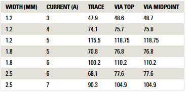
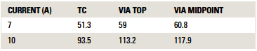
The comparison is even more dramatic if we simulate a 2 oz. trace. Just for fun, we looked at a 2.5mm, 2oz. trace carrying 7A and 10A (TABLE 4). Note that with 10A the via midpoint temperature is about 118˚C, almost 25˚ hotter than the trace. But consider this: A single 0.66mm trace (with the same cross-sectional area as this via) carrying 10A would reach the melting point of copper (1083˚C) in approximately 7.5 sec!6 The via only reaches 118˚C because of the thermal coupling to the 2oz. trace.
Table 4. Results of a Simulated 2.5mm, 2oz. Trace at 7A and 10A
Conclusions
It would be tempting to conclude the via dimension doesn’t matter. The trace controls the via temperature because of the thermal coupling between the via and the trace. We do not go that far. But the primary conclusion from all this is that vias can carry much more current than previously assumed. This explains why via failures due solely to temperature are so rare. Common wisdom has been that the via should have approximately the same cross-sectional area as the trace. For larger traces, multiple vias should be used to keep this equality. But the results from these simulations show that the following rule is approximately true instead (at least within reasonable limits): It is not the current that determines the via temperature. The via temperature is determined (at least approximately) by the trace temperature.
The reader may wonder about the air-filled cavity in the via core. This has no appreciable impact on via heating or cooling. The cooling of the via is through the dielectric and through thermal conductivity with the trace.
But what if we filled the via core? If we filled it with solder, there would be only a minor impact. The resistivity of solder is at least 10 times that of copper, so most of the current would flow through the wall of the via anyway. Therefore, the heating and cooling characteristic would be largely the same. If we filled it with copper, the resistance would be lower so the I2R heat generation would be less. Therefore, the thermal performance would be better. Similarly, a larger via with the same plating, or the same via with thicker plating, would also perform somewhat better.
References
1. Douglas G. Brooks, Ph.D. and Johannes Adam, “Trace Current/Temperature Relationships,” PCD&F, June 2015. A more comprehensive analysis, “Trace Currents and Temperatures Revisited,” and “Fusing Currents in Traces,” is available at ultracad.com. This article is an abbreviated version of a longer paper, “Via Currents and Temperatures,” also available from the UltraCAD website.
2. Throughout this paper, whenever we use the term “via cross-sectional area” it should be understood that we mean the “via conducting cross-sectional area,” the cross-sectional area of the copper wall.
3. IPC-2152, “Standard for Determining Current Carrying Capacity in Printed Board Design,” September 2009.
4. TRM (Thermal Risk Management) is designed to analyze temperatures across a circuit board, taking into consideration the complete trace layout with optional Joule heating, as well as various components and their own contributions to heat generation. Learn more about TRM at adam-research.com.
5. A 10 mil diameter via with a 1.0oz. (1.3 mil) wall has a cross-sectional area of 35.5mil2, equivalent to a 27.3 mil wide 1.0oz. trace.
6. See Douglas Brooks and Johannes Adam, “Fusing Currents in Traces,” ultracad.com. The calculation was made with UltraCAD’s UCADPCB4 Trace Calculator.
Douglas Brooks, Ph.D., is owner of UltraCAD Design, a PCB design service bureau and author of PCB Currents: How They Flow, How They React; This email address is being protected from spambots. You need JavaScript enabled to view it.. Johannes Adam, Ph.D., CID, is founder of ADAM Research, a technical consultant for electronics companies and a software developer, and the author of the Thermal Risk Management simulation program.


