SAN JOSE, CA — Avishtech has announced the launch of two new low-cost toolsets, Gauss SI and SI PRO, that are designed to provide a clear and easy-to-use pathway to rapidly construct PCB stackups and quickly simulate for impedance and loss.
"While Avishtech’s primary purpose with our flagship Gauss Stack software is providing a fully integrated solution that allows Computational Prototyping for reliability, manufacturability, and signal integrity, at a fundamental level, designing a stackup from a library of materials and simulating for signal integrity is almost as critical as the layout," said Keshav Amla, founder and CEO of Avishtech. "Up until now, even these capabilities were only available to large corporations, who could afford very expensive software, such as our Gauss Stack or some other offerings in the market. However, we feel that every board designer and engineer should have the ability to specify their stackup and design for impedance and signal integrity and that’s why we’ve launched this new offering."
Emphasizing the importance of addressing the stackup design process for today’s high data rate, high frequency designs, Avishtech will feature leading PCB industry expert, Lee Ritchey in its booth (913) at DesignCon on Feb. 1-2.
"Starting with traditional stack-up design, the primary concern was getting the impedance right and having enough layers to hold the signals. So, most engineers put the burden of getting the impedance calculation right on the fab shop.," Ritchey said. "Hidden from view was that the fab shop engineer dealt with all of the manufacturing issues. With modern board design there are several other issues that must be accounted for including path loss, skew and very complex power delivery engineering. None of these are fab engineers capable of dealing with. As a result, the SI engineer has to take charge of the stackup design. Now, the SI engineer has to be the one responsible for manufacturability issues such as resin starvation, via reliability, glass stop, etc. This is what Avishtech’s Gauss Stack addresses."
For the foregoing reasons as well as several others, Gauss SI and Gauss SI Pro have built-in intelligence to make the stackup process easier, more accurate and better optimized.
"Unfortunately, stackup design as a discipline within the product development process is not taught in most universities," Ritchey said. "As a result, product developers can be intimidated by the task just because they have not had a lot of experience with it. They learn stackup through ‘on-the-job’ experiences and, along the way, they understandably tend to make mistakes. With today’s high-speed products there is very little room for errors or inaccuracies so ‘what if’ analyses becomes a critical part of the process and that process is not always readily understood. Avishtech’s toolsets are easy to use and provide a level of predictability and reliability that is not available with any other solutions being offered today."
Key features and benefits of Gauss SI and Gauss SI Pro include:
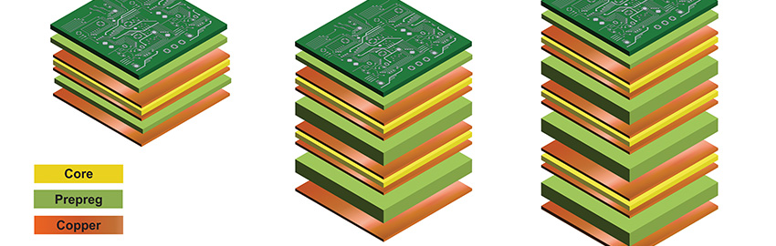
- An extensive, built-in dielectric materials library that enables product developers to specify each layer of a PCB stackup within seconds.
- Static or frequency-dependent Impedance and loss analysis and synthesis for all transmission lines with a single click.
Additional capabilities and features for Gauss SI Pro include:
- S-Parameters analysis, viewing, and export.
- Frequency-dependent properties analysis, viewing, and export.
- Uncertainty Analysis to account for the impact of manufacturing tolerances on impedance and loss.