For students at Palomar Community College, a finely-tuned design curriculum is just the beginning.
It goes without saying that finding talent is a big deal in electronics hardware development. Outside of internal training programs, talent development falls to the handful of colleges, universities and third parties involved in teaching printed circuit design and manufacturing.
One of the original providers is Palomar College, located in San Marcos, CA, part of San Diego County. The community college has offered practical printed circuit design coursework since the mid-1990s.

John Watson is teaching a full-year PCB design class at Palomar Community College.
John Watson's day job is customer success manager at Altium. But twice a week during the school year, he teaches the course on printed circuit design at Palomar. He spoke with us in May for the PCB Chat podcast. This transcript of that interview is lightly edited for length and clarity.
Mike Buetow: As I understand it, there are two segments, printed circuit board design and advanced printed circuit board design. Give us a sense of what you cover in those courses.
John Watson: There's no background students are required to have, or any prerequisites. These are brand new designers. That's where I start things. With the basics class, my main objective is to walk them through the entire PCB design process. I have 16 weeks to do that. It's a really good chunk of time. I conduct class twice a week in the evenings. It is an online class, which makes it convenient for a lot of students.
In this class, we focus on the four stages of the PCB. We start with libraries, where we talk about the library structure, the component structure, things like that. The second stage is the schematic. From here, it's a linear process that we walk students through to create their own – and usually their first – PCB design. They go through the schematic, then we push that into the PCB, and then go into the documentation stage, where we output everything – Gerber packages, fab drawings, assembly drawing and so on. Our main focus on that class is to get them through that process from start to finish. Like I said, it's a very linear process, so we build on what we did the previous week, and say, "OK, now that you've done this, you now can do this next step."
In the advanced class, which is another 16 weeks, we pick up from where we created our document package and then we actually go into the fab and assembly processes. I think this is an area that a lot of times is missed by designers. I work with a lot of fabricators and assemblers in the area, and I've asked them, "How many PCB designers actually come and visit a fab house?" It's actually very, very low. I would encourage PCB designers to visit a fabricator, and understand how this all comes together. You'll have a much better understanding of printed circuit board design. It's really, really an interesting concept and process that they go through.
Let me go back one step here in our basics class. We actually design a controller board from the Mars Rover that we give to the students. That's their PCB project that they're working on throughout that semester. In the advanced class, we then look at three PCB designs, so we focus more on the PCB side of this and the layout side, because what we developed there is a much deeper dive into the PCB process. For the fab and the assembly process we visit a fabricator. We see the assembly process, we see the machines and the steps taken by the fabricator to take our data and create the board, and bring back to us a completed design.
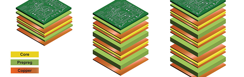
The second stage of the advanced class is rigid-flex design. This is an amazing area. I think it's one of the faster-growing areas of PCB design, especially with all the wearable medical devices; products like this really have driven that entire industry. For four weeks I concentrate on rigid-flex design, and it's exciting to watch your students do that PCB. We then go into advanced PCB design, working on a BGA design; a rather big one. This now involves all those different important physics of electronics: EMC, EMI, link tuning, skin effect, and we talk about why things happen in the PCB in the way they do.
In the basics class I'm more concerned about students connecting the dots: "Let's solve the puzzle that you have in front of you." In the advanced class we look deeper into why a trace will be this length or why we need to have protection for EMC and EMI. I go a lot into the physics of a trace and the printed circuit board itself to understand why certain things are done, so they have a much broader picture of exactly why they should do things. For the last section of the advanced class we take the three PCBs we've done and put them together, and we actually build a system design. Now we're talking about system configuration, system design, harness design, things like that. We also get into more of the MCAD collaboration where we're looking at the role of the entire team and who is involved with what deliverables. Students now work together as a team on that final project.
Between the basic and the advanced classes, I have 32 weeks, which I will tell you is not enough. I was recently talking to a professor and department head at a major university about the program and they asked, "How long do you teach just PCB design?" I said, "Thirty-two weeks." And they go, "Wow, I do six weeks." What do you teach in six weeks? I barely scratch the surface. But this is a phenomenal program.
MB: Do you get into impedance control, transmission lines, things like that?
JW: Absolutely. And we tie this into the physics of it. We say, "If you have a trace of this length, what are we talking about here?" Because of the copper formation and the atoms and the free electron sitting out there that basically gets kicked around by everybody, we can now start developing from those basic physics principles some other things. I go, "So if this is true, then let's look at how this affects our layout. If we have a trace of this length, we can determine there's a set impedance." We talk a lot about single line impedance. We also talk about differentials, and why and where they're used. We get into length tuning. Then we get into the energy of the trace when we talk about EMC and EMI and how we control them. We look at the PCB in really, really deep detail in that advanced class, where we look at it and we say, "OK, there are some things here we like to control. We use these principles to benefit our design." Let me give you an example. When we're talking about differential pairs, we actually love crosstalk, right? We want crosstalk. But when we're talking about high-speed design, we don't want that. Having the students understand why certain things are used and how they are used, they begin to see a PCB in a different light. They don't see it as just solving the puzzle and making the connections. They look at it as an engineering, almost a mechanical, item. With the development of the PCB design, it's understanding the physics of it all. And that's exactly what I tried to bring to the students.
MB: You mentioned that the class is taught online. Is that a concession to Covid that's been carried over?
JW: Yes, and it's really been beneficial for us. I've enjoyed teaching it online rather than in the classroom because now what is happening is I can have a student who has a question share their screen, and we can walk through it as a class, watching the screen, which really makes it beneficial for everyone. Otherwise, if I was in a classroom setting, I'd have everyone gathered around the computer and peeking over each other's shoulders.
MB: You do a visit to a fab shop, but if this is online, how do you? How do you replicate that?
JW: The one time we come together as a class is that tour of the fab house.
MB: And if the students aren't located within a reasonable drive, do they sit that one out, or is there some other way that you try to convey that information?
JW: I can't record the tour, because it is an ITAR-compliant facility. But I have videos of the process from other tours. I have them look at those (videos) and, with my out-of-state students, I actually go visit them at some point. I've gotten into the habit to meet my students face-to-face. I want to find out why they are taking this course. That's usually a question I ask them the very first night: Take a piece of paper and write why you're doing this. I find that such a great motivator for them later, because I tell them, "This is not going to be an easy class. This is going to be very difficult if you've never done this before, and you're going to find this frustrating. Sometimes you're going to pull your hair out. I want you to write down why you're doing this, and then when you get into those situations where you are frustrated, pull that sheet of paper out, reread it and refocus yourself on why exactly you're doing this."
That's the principle we want to try even in the careers we have now. I do it in my career, to understand why I'm doing something.
MB: You're taking home-schooling really literally. Sounds almost like Mr. Hand showing up at Spicoli's house in Fast Times at Ridgemont High.
JW: I have come into this through the industry. I'm not a professor. I didn't go to school and say, "I'm going to be a teacher." As a person who's been in the industry for 43 years in electronics, and 23 of those in PCB design, it was something that I love doing. I don't just say, "Read this chapter and take a quiz." I bring real-world exercises and experience into this. I run my class the way I would run a company. As example, I will have students doing a PCB design or their lab working on their designs, and all of a sudden I'll say, "We just got a phone call from the sales department saying we have to cut $50 out of our bottom line. What do you do?" And you know, you hear the shrieks going up through the class. But this is real. I'd love to start a PCB design and everybody leaves me alone and nothing happens. There's no challenges and I just work through this whole process and it comes out the other side and goes to fab and it's all perfect.
MB: Good luck.
JW: Remember the old Atari video game called Pitfall? You're running through this jungle and the whole jungle would open up and you'd fall into this pit. And that's PCB design. That's how I described this to my students. It is like you're running a gauntlet of issues and problems and you try to keep control of it. But it's, how do you control that and what affects your design? This is how I teach it: "You have this issue. Now where do we go? What's our first step? What's our next step?" and so on. One of the traits I give students is, "You will be successful in this course if you learn to eat the elephant. Take it one step at a time, one bite at a time. Don't get frustrated by it and you'll get through this." It's all done one step at a time. Understand what affects other things.
I really have a mixture of students. By the way, in my class I have EEs who are training for an EE degree. There's that level in the college system. There's also new PCB designers looking for career changes. That's probably one of the most interesting areas, because you would think that EE should have this all down. I actually find that the EEs have more of a problem with PCB design.
MB: Why is that?
JW: I think it's because they get too much into the details and lose their focus on the solution. The best way I can describe this is they will lay down the trace, for example, and they say, "Was that right?" The better question is: Is it a solution? I give each one the same schematic when they start, but I tell them every one of your PCBs is going to be different. What's unique about PCB design is the artistic side, where your individuality comes out in the design.
A lot of times I find that EEs have to look at it in a deeper sense. I've seen in my career that some of the best PCB designers are artists. People say you can't teach that side of it, it's something they have to see for themselves. It's where they see a solution. They see the PCB and visualize how this can come together.
MB: I do think that understanding or thinking in three dimensions helps a lot. Another colleague suggested that the future of PCB design is playing Minecraft right now, and I don't think she's wrong. It teaches you to think in three dimensions and not think of everything as a flat object, and particularly now the way that designs are going, there's so much connected. You have to think of the chip and board almost as a single object, to consider more than just this trace on this plane.
JW: Right. And we definitely get into that with the advanced classes when we start developing our layer stacks. The basics class (designs) a four-layer board. When we get into the advanced class, we're looking at eight and 10 layers because we're talking about a rather big BGA and they have to think, how do I formulate and put this puzzle together in much more of a broader sense?
When I take the students through the process, especially when we make the jump from the schematic to the PCB, I don't tell them what's going to happen. It's like, "OK folks, we're ready to jump from our schematic to our PCB. Go ahead and here's your process and we're going to push this." I take a step back and watch and they push their schematics in their PCB and all of a sudden it's like "holy smoke!" with all the connections and the components and the rats nest going everywhere. I love the fact that we can take these students and bring them through this process. I really think our industry needs this, and that's really what drives me. I've noticed for close to 10 years now, there is a downturn of available talent in our industry. I get calls every week from companies saying, "Are you available for work we have?" There is a real lack of talent in our industry and this has been a growing trend for at least 10 years. PCD&F does the yearly survey of PCB designers and they ask, "Do you intend to retire in the next 12 months?" Those percentages have been in the high 50s or low 60s for some time now. I did a presentation where I asked the audience, "Has anyone else heard the massive sucking sound coming from companies? It's the talent that's walking out the front door." Those designers that walk out with all their years of experience. It's something that I've seen for some time. When I had the opportunity to step in and reverse that trend, I grabbed it. Palomar College is one of the only colleges in the nation that offers PCB design at this level: 32 weeks. Most of the universities offer, at most, eight weeks of PCB design. It's one of those areas that we can take advantage of.
I have the college here working with companies saying, "If you need individuals for internships, we would love opportunities for our graduates." I have several students that have recently gone through my advanced class that were referred to me from their (employers). They go back to their company, and now they're in a better position.
MB: How many students take the basics class and then don't take the advanced class?
JW: About 70% from the basics go on to advanced. There is a drop. I'm working on opening the advanced class to those who are experienced designers. It's been requested a lot by individuals who know PCB design and would like to take the advanced class without the basics course as a prerequisite. Under the discretion of the professor, we can accept students into the advanced class. I'm going to be looking at it for spring semester 2024, which starts in January.
MB: Here's a key question. Do you teach hand routing or autorouting?
JW: I do not teach autorouting. First off, I don't see auto routing as a popular thing in PCB design. I would love to ask industry-wide how many designers autoroute PCBs. (I think) you'll find that the percentage is very, very low.
If someone is familiar with PCB design, they say, "Can I autoroute my board?" I would prefer not. The reason is, I want them to learn this process. My goal is to teach the students critical thinking. And when you just push the button and go get your coffee, there's a couple problems. One is, you're not involved in the PCB design process. You've stepped away. You've let it run its course through the AI of the program. From what I've seen, this is not popular in our industry because it pulls you out of the design process. I find that people do PCB design because it's the solving the puzzle, the creative process, that they want to do. Autorouting completely takes you out of that. So no, I don't teach autoroute. I teach them hand routing of boards. Now, I will bring in some of the active routing or the intermediate routing techniques that you're not just laying a trace down from point A to point B. There's some tricks on the tools themselves that are not autorouting but will help you to improve your routing techniques and still keep you in full control of the route process.
MB: That's fair. To what extent have you been able to modify or add to the curriculum? Have you been able to put your own personal stamp on it?
JW: Oh yeah, as a matter of fact, my curriculum is very fluid. I talk to companies about what they need, what technologies they're bringing in and developing, and from that I massage the curriculum each year, to focus on what companies are looking for in these special technologies. As we know, it's constantly changing in our industry. I think we're seeing some of the greatest innovations we've ever seen in our industry right now. Unbelievable innovations. I have to constantly keep looking at it and say: What do I change? What do I keep improving on? That's a major part of what I do, especially outside of class. An individual who came into my basics class was a janitor who wanted a career change. He went through the basics and the advanced class having never (previously) done a PCB design. Now he works for a company in Carlsbad as their junior PCB designer. I developed my curriculum from the companies. I then work with those companies, saying: "Here is an individual who has learned what you want him to learn, and give him an opportunity and open up an internship or a job."
MB: I love that about community colleges. With four-year institutions, one of the metrics is "X percentage of our graduates have a job within six months." That's important. College is a huge investment of time and money. But community college is all about being employed, learning how to do something and put it into practice. And if I look at Zippia, the most common academic background for PCB designers in the US today is an associate's degree. Palomar is in the sweet spot in that.
Palomar is really punching above its weight when it comes to design, and there's also classes on geometric tolerancing and dimensioning. There's multiple classes on 3-D design using SolidWorks. Whether you're into electrical or mechanical, it seems like there's something for everyone.
JW: Oh absolutely. And that is something that we are known for at Palomar. Just looking at San Diego, for example, you will have specialty areas in each of the community colleges. Here, Palomar College is quickly becoming known for its engineering; if you want to learn engineering, our college is your place to go. And yes, we have programs that are not just for development but now also this manufacturing side; we're now looking at CNC milling and the mechanical and all these other disciplines in the design process, which is phenomenal. I'm looking forward to the time though, that we as a college could develop a kind of a system or a college project. We are all working in our own areas. We could come together and work as a college toward a single project of some kind that would involve all these different disciplines. That's what we're looking at doing in the future.
Table 1. PCB Designers Educational Background (Source: Zippia)

MB: To that extent, Lorraine Community College in Ohio offers an SMT or an advanced assembly program for electronics, and they have built it to the point now where it's a bachelor's degree offered from a community college. The program is tied into local OEMs and assemblers who will effectively sponsor future employees. They're not their own employees, but they will say, "We have a need for five more people. So if you graduate five people in the next three years, we guarantee that we'll have a job for those folks." A very interesting model, but it does have a hard cap insofar as the number of students that are available to go through the program at any given time. With the Palomar design courses being online, the opportunities are much broader. And because you don't have the same kind of equipment constraints – you don't need an SMT line in your bedroom in order to learn this – there's a much broader potential reach. Do you have a cap on the number of students? There's a point where there's going to be diminishing returns. If there are 50 people in the class, you're not going to be able to do everything you can if there's 25.
JW: Exactly. We are capped for a class at 22. I usually shoot for 25. There will be a few dropouts at the very beginning, but each class can have 25. If, for example, my first class fills up and I have enough people on a waiting list, I could then approach the college and say we'd like to conduct a second class. These could be done on alternate nights of the week. That is an option.
Last year at this time, they were looking at canceling this class entirely. I spoke to the dean and told them that would be a very bad mistake because we are in an industry that needs these individuals. The need is there, and I took the challenge of filling this class. One of my major undertakings is not just to fill this class but also fill the waiting list.
This is the need is there, it's just a matter of getting the word out that this is available. You don't need a prerequisite. You don't have to have an EE. You don't have to have special training. I've seen individuals come from every area of life into this industry. I came up as an electronic technician. But you can do any path you wish. That's what's amazing about this.

Figure 1. PCB designer unemployment rate by year.
MB: Yeah, the unemployment rate among PCB designers in the US is less than 2%. If you can do PCB design, you will be hired. I'll go back to Lorraine Community College for a moment. One of the things their director told me was that they've offered to license the program to other junior colleges around the country and have seen no interest. Has Palomar talked with other community colleges, or even for that matter, other four-year institutions about packaging this coursework and offering it in some shape or form?
JW: Yes, yes, we are looking at getting this course certified by the state right now and then any community college in California, at least to start, will be able to take this course and get credit for their own college. We are in that process right now. I get students from those colleges who are attending for the sake of learning but not getting college credit. We would like to be able to have them get college credit. The steps I need to go through with that is to get my course certified by the state community college system and then it will be accepted. Because it's online, it makes it convenient. Anybody, anywhere in California will be able to take this and get college credit.
Ed.: Palomar's DT-226 Basic PCB Class is scheduled to start Aug. 22 (https://palomar.programmapper.ws/academics/interest-clusters/dbe0f8d1-c2e1-450f-afa3-661d42bfc243/programs/536f5d77-4fde-47c1-6435-4d607d902c2f). The Palomar website is palomar.edu. Prospective students may contact Watson at This email address is being protected from spambots. You need JavaScript enabled to view it. or This email address is being protected from spambots. You need JavaScript enabled to view it..
Watson will also take part in a free panel on Next-Generation Engineers on Sept. 20 at PCB West (pcbwest.com) this year.
Mike Buetow is president of PCEA (pcea.net); This email address is being protected from spambots. You need JavaScript enabled to view it..