Wafer-level packaging packed the record house.
A record crowd of more than 1,500 people representing 32 countries attended the Electronics Components and Technology Conference (ECTC) in San Diego to attend short courses, listen to more than 360 presentations, and discuss the latest trends. A special session examining sustainability in microelectronics started the conference with discussions from academics and industry. The panel on advancements in bio-med technology and associated packaging provided key insights into today’s cutting-edge research in medical developments ranging from sweat sensors providing diagnostic assistance to brain implants controlling conditions such as Tourette Syndrome. Evening sessions stirred lively discussions on hot topics such as nano packaging, the Internet of Things (IoT) and the future of interconnected electronics, and cooling for high-performance systems. A special women’s panel provided great advice for everyone on the road to professional success, regardless of gender.
The most heavily attended sessions (and short courses) discussed fan-out wafer-level packages (FO-WLP). In one session 273 people practically stood on top of each other to hear the latest developments. Stats ChipPAC provided additional details of its WLP in reconstituted wafer format. A presentation from Fraunhofer IZM and the Technical University of Berlin outlined progress in large area compression molding for FO-WLP. ASE described its fan-out technology for a WiFi system-in-package (SiP) module. Nanium released reliability data for large die (25 x 23mm) for fan-in WLP applications, amazing attendees.
Sessions were also standing-room-only to hear the latest discussions on flip-chip assembly from all sides of the supply chain, including presentations from Amkor, ASE, SPIL, Qualcomm, Samsung, GlobalFoundries, TSMC and UMC. Especially interesting were presentations focusing on flip-chip assembly for the next silicon technology nodes, including 20nm and even 14nm. As the industry considers the implications for connecting ICs fabricated with ultra low-k (ULK) dielectrics, concerns increase for chip-to-package interaction (CPI). Given the forecast for narrow bump pitch (≤100µm) and increased use of Cu pillar bumps, many companies plan to use thermocompression bonding (TCB).
Presentations articulated the elevated CPI risk associated with critical issues of circuit design, silicon processing (such as BEOL/FBEOL) and steps in the packaging and assembly process such as singulation, chip-attach and encapsulation, and material properties such as Tg, CTE, and modulus. Large die size and the ratio between ULK and low-k have been found to be a major factor in increased CPI risk. The goal is to minimize stress at the interface with the ULK layer. Several papers discussed the careful attention required for bond force and temperature, selection of underfill material and assembly processes.
Investigations of assembly with nonconductive paste and nonconductive film gave attendees better insight into the possibilities of new material solutions. K&S discussed its new flip-chip bonder, and ASM introduced its latest product, discussing the merits of flux-based and fluxless assembly with TCB. New TCB systems are focused on increased throughput. Additional information on the latest in flip-chip assembly equipment was provided by such exhibitors as Amicra, Finetech, MRSI, Panasonic, SEC, SET, and Toray Engineering.
Interposers: Quiet but steady progress. While the interposer sessions were not as packed as in past years, attendees heard the latest developments in silicon and glass interposer fabrication, and several exciting advances were revealed.
Xilinx presented its reliability evaluation of the largest interposer published to date: a 25 x 45mm silicon interposer assembled to a 55 x 55mm organic package substrate. The TSMC CoWoS process is used for the assembly. Warpage was found to be acceptable, and in unbiased HAST, the package passed 2,275 cycles.
Powertech Technology described a chip-on-wafer process for high-end CMOS image sensor applications.
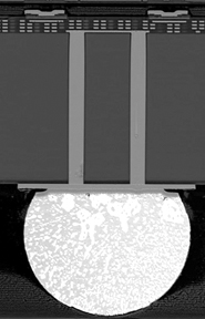
IMEC described its latest achievements in engineering improvements to handle stress and bowing of silicon interposers. Progress in TSV fill was discussed by TEL-NEXX, and Lam Research introduced its backside via reveal process for a via-middle process flow. GlobalFoundries revealed more of its work on interposers, including detail of its research into a room-temperature atomic layer deposition line for TSV applications and reliability data for backside probing of a 50µm thin TSV wafer (FIGURE 1). GlobalFoundries reported increased interest in its interposer offerings and announced a close working relationship with Amkor to provide a full supply-chain solution. Renesas presented work on a low-cost, single-sided silicon interposer targeted for mobile applications.

Figure 1. A close-up view of an interposer and TSV.
Asahi Glass, Corning, Georgia Tech and RTI International reported progress with glass interposers. Organic interposer developments were also covered. Ushio reported on fabrication of an ultra-thin organic interposer. IBM reported on assembly of large die on organic interposers.
3D IC and alternatives. The market for 3D ICs with through silicon vias (TSV) is focused on high-performance applications. Stacked memory with TSVs continues to move into production with shipments from Micron, SK Hynix and Samsung. While there were no earthshattering announcements of new applications for 3D ICs, several presentations reported on process improvements. In mobile applications, package-on-package clearly remains the primary choice for high-performance application processors and memory. Several presentations focused on new PoP developments, including methods to reduce warpage.
New developments on MEMS and sensors were also highlighted this year. A session on wearable, bendable and flexible electronics included presentations on e-textiles, blood analysis systems, and new materials such as anisotropic conductive films (ACF) and other new adhesive films. NAMICS introduced a new insulating adhesive film for high-frequency wearable electronics. Dow Corning introduced its new thermal interface material, a one-part silicone gel with a thermal conductivity of 4.3W/mK. The material was developed in conjunction with IBM as a TIM1 solution.
Advanced optical interconnects were discussed both by universities and companies such as Altera, Fujitsu and IBM. Another session focused on silicon photonics and light sources with presentations from IBM, Philips, Oracle and the Photonics Electronics Technology Research Association, as well as a number of universities from around the globe. Sessions also covered lead-free developments and emerging interconnect developments.
Packaging and assembly - the new value-add. With the explosive growth in connectivity, data transfer and storage, and data processing, driven by whatever we choose to call it – IoT, Internet of Everything, or some other yet to be invented term – the package is becoming a value add! Leading companies in the application space are focused on the critical importance of package and assembly early in the design phase of the product and the enablement of the total system solution.
There is a high degree of predictability in silicon node roadmaps, even as they become increasingly expensive. Predicting the next wave in packaging trends is becoming much more challenging because there are a growing number of choices with more than just technical tradeoffs to consider. Understanding where the packaging and assembly trends are heading requires a skill as honed as reading the changing directions of the wind on the water while sailing the San Diego Bay. Charting the course without allowing the sails to luff wins the race.
E. Jan Vardaman is president of TechSearch International (techsearchinc.com); This email address is being protected from spambots. You need JavaScript enabled to view it.. Her column appears bimonthly.


