
Will economics drive the next round of package innovation?
Performance was the main driver for semiconductor packaging and assembly developments in the early days of electronics, but in the past two decades the demands of miniaturization have spurred development of many new package concepts. As we move into the next era of electronics, economics is also expected to play an increasingly critical role.
Starting with military electronics and segueing into computing, improved performance (and reliability) has been paramount in the development of each new generation of semiconductor package. Semiconductors for military applications were assembled in ceramic packages. Providing both electrical and thermal performance solutions was the key to product success. High-performance computing requirements led IBM to the development of multichip modules such as IBM thermal conduction module TCM with 101 layers of glass ceramics and a multitude of flip-chip devices.
As the PC era was ushered in, computers began to appear on every desk, at work and in the home. Performance requirements drove the move from wirebond to flip-chip for CPUs. IBM licensed its flip-chip bump evaporation process to AMD and Motorola. Intel, with a cross-licensing agreement, internally developed a plated flip-chip process. While performance was important, new lower-cost solutions were needed to meet the goal of computing industry democratization. Intel initiated the shift from ceramic to laminate substrates for its flip-chip CPUs. The first packages were pin grid arrays (PGAs), but this has gradually shifted to greater adoption of plastic ball grid arrays (PBGAs). For PCs, a high-volume application, a strong supply base for flip-chip organic substrates developed. While Intel’s assembly took place internally, companies such as LSI Logic, relying on subcontractors, licensed its flip-chip assembly technology to a number of OSATs, creating an infrastructure available for all. Supply chain expansion and industry infrastructure development permitted the growth of packages with laminate substrates, and the industry moved from the ceramic age to the age of organic substrates.
The development of chip-size packages (CSPs) enabled the introduction of handheld digital camcorders, cameras, and small, lightweight mobile phones. Form factor became an essential parameter for these products. Reduced package footprint on the board was a major goal. In a strict definition, the package could only be 1.2 times the size of the die. Many CSP versions were introduced: some with leadframes, others with flex circuit or laminate substrates, and eventually a wafer-level package (WLP) in which all the packaging was completed while the die was still in wafer format, before dicing.
Thin is the fashion. Mobile phones, specifically smartphones, represent the industry’s highest volume product – driving today’s semiconductor package shipments. Fashion dictates these products are made thinner and thinner, driving greater use of WLPs and the introduction of thinner package solutions. Apple’s first iPhone used two WLPs, but the much thinner iPhone 6 has more than 26 WLPs. Even the latest portable communication gadget, the Apple Watch, contains nine WLPs. The CAGR for fan-in WLPs in units from 2014 to 2019 is almost 9%, while the CAGR for wafers is 10%.
In 2007 a new type of WLP was introduced by Infineon and used to package baseband processors. Creating interconnect on top of the die placed in a reconstituted wafer format permitted a package structure that could handle higher I/Os, as the move to advanced silicon technology nodes provided die shrinks.
An increasing number of companies are adopting fan-out WLPs (FO-WLPs) for PMIC, RF and application processors, as well as controllers, media chips and sensors. Multichip versions are shipping for radar modules in automotive applications. Amkor recently announced it would redeploy its production of an FO-WLP program on 300mm wafers. Amkor’s original work several years ago was on 200mm. This latest move is based on demand from customers. Much of the FO-WLP structure is the eWLB-type process originally introduced by Infineon’s wireless division (purchased by Intel). Amkor joins a growing list of suppliers for FO-WLP that includes ASE, Deca Technologies, NANIUM, NEPES, SPIL, STATS ChipPAC, and TSMC (with its InFO process). FlipChip International has been acquired by Huatian Technology, and has an FO-WLP based on WLP embedded in flex circuit. Additional companies are expected to join the list of FO-WLP suppliers.
Package-on-package (PoP) development was driven by consumer product and mobile device requirements of close connection between memory and logic. A memory package is mounted on top of a logic package (typically an application processor). The first PoP reported in teardown reports at the beginning of 2005 had three memories in the top PoP and a total package thickness of 1.8mm. By mid 2006, a 1.4mm package height was reported for the same number of die.
Package heights continued to decline to 1.2mm in 2012. Package thickness will continue to decrease, with a target thickness of less than 1.0mm and even 0.8mm on some roadmaps. To reach the goal of ≤0.8mm, some companies are expected to use an FO-WLP for the logic device in the bottom PoP.
System-in-package (SiP) is also gaining in popularity. While there are different views on the definition of SiP, a basic definition is one or more devices with passives that provide a standalone function. SiP can take the form of FBGA, FLGA or even a leadframe package. Several companies are investigating FO-WLP as an SiP solution. Freescale Semiconductor and NXP have announced FO-WLP SiPs for radar modules, enabling improved automotive safety features. A variety of SiPs are expected to see rapid growth in wearable products, as demonstrated by the introduction of SiP as an enabler of Apple’s watch. The ability to combine many devices into a package meeting performance, low profile, and economic demands will be an enabler of new wearables.
As explained by ASE’s Dr. William Chen at a recent IMAPS wearable electronics workshop keynote, heterogeneous integration in the form of SiP could be the answer to dealing with higher cost of next node semiconductor fabrication. SiP permits more complex devices to be packaged close together. SiP is expected to enable the integration of many devices into a small form factor with improved performance.
Is ‘printed’ the future? The application of new manufacturing methods and materials may be required to meet future cost-reduction demands. There is great interest in the possibility of printed electronics for new circuit applications, and many companies and organizations are working on development of new materials and technology. 3D printing holds near-term possibilities for cost-reduction. One example is in conventional leadframe packages such as QFNs, a mature technology for which costs would be difficult to further cut under existing conditions. EoPlex, headquartered in San Jose, has demonstrated use of mezoscale printing to fabricate a QFN package that is significantly thinner (down to 40µm thick), with 60% less weight, and potentially with a lower cost than an existing QFN. In the process, 3D printed package components are fabricated on a stainless steel carrier that is removed to leave pad for interconnect (FIGURE 1).
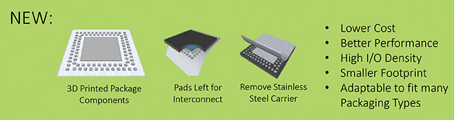
Figure 1. 3D printed package components on peelable stainless steel carrier created with CSI platform. (Source: EoPlex)
As companies ponder the extreme costs associated with the fabrication of next-generation silicon nodes, packaging and assembly developments may provide the critical cost-reduction required to create the products of the future. New innovative package designs, new materials, and greater cooperation among all participants in the supply chain are anticipated.
E. Jan Vardaman is president of TechSearch International (techsearchinc.com); This email address is being protected from spambots. You need JavaScript enabled to view it.. Her column appears bimonthly.


