Key aspects of ATE platform boards and how an IPC test panel design is used to qualify suppliers.
ATE platform boards are simply defined as interfaces used between a semiconductor device and an electrical tester. They include necessary circuitry for device testing and can also dock to a robotic handler for running high-volume production. Handler applications vary, generally manipulating either a semiconductor wafer (probe test) or an IC device package (final test).
Development stages of an ATE board include design, fabrication and assembly. The challenges and significant characteristics of making ATE boards put them into a distinctive category in PCB manufacturing. Some common considerations of ATE board fabrication include:
Via aspect ratio. Typical ATE board thickness requirements range from 0.125" to 0.250" (3.175 to 6.35mm). This board thickness is used primarily for mechanical stiffness. High layer counts are necessary for some test solutions, which results in a large board thickness in addition. The number of layers within an ATE board can be greater than 40.
The substantial thickness of an ATE board leads to electrical interconnect vias having a high aspect ratio. (Aspect ratio is defined as a via’s drill depth over its drill diameter.) As via aspect ratio increases, it becomes more difficult to achieve adequate copper thickness plated along the hole wall, especially at the barrel center.
Sequential lamination. Many PCBs are manufactured with only one lamination step (or press-cycle) to fuse all its layers together. Sequential lamination involves creating two or more multilayer boards first and subsequently pressing those together to form a single board.
Complex builds may require additional lamination cycles and might also use microvia buildup layers. This can lead to a particular board section undergoing two to five cycles in the press. Multiple lamination cycles are common for ATE boards. Reasons this is incorporated include aspect-ratio reduction, limited drill-bit flute lengths, and microvia buildup layers.
Multiple lamination cycles can cause a board to be more susceptible to delamination. Board delamination may not be apparent until after a component assembly reflow cycle or perhaps upon inspection after failure in the field.
Registration. Registration is loosely described here as the vertical alignment of PCB features on different layers. It is a critical aspect for attaining layer-to-layer electrical interconnects. Misregistration occurs during the PCB build process for numerous reasons. High layer counts, multiple lamination cycles, small PCB features, and errors compensating for material movement (that occurs during lamination) all contribute to the likelihood of registration failure.
While often viewed as a consideration for achieving a desired electrical interconnect, registration can also be thought of as an amount of drill-to-copper clearance necessary to maintain a desired electrical isolation. Drill wander is a separate issue, but its net effect results as a misregistration problem as well.
Multiple PCB features and technologies. ATE board designs can require multiple PCB features, feature sizes and process technologies. In that case, a fabricator must be capable and proficient with all. Specific technology requirements might include laser microvias, blind and buried vias, fine lines and spaces, backdrill through-holes, vias plated shut, partial-depth via plugging, selective NiAu finish, and very high layer counts. Other ATE board requirements can also involve atypically low tolerances for controlled impedance, positional accuracy, bow and twist, and relative copper feature height.
Resilience to mechanical and thermal stresses. Electrical interface to ATE boards is generally accomplished using spring-loaded pogo pins, which can number in the thousands on a given board, exerting a minimum of 25g of force per pogo pin. Pogo pin forces occur at both the electrical tester interface and the interface to the device(s) under test.
Docking to a robotic handler can also exert substantial forces on an ATE board. All these mechanical forces are typically dealt with using a combination of board thickness, metal stiffeners, and support plates.
Of even greater concern are the temperatures at which an ATE board might need to be subjected. Semiconductor device testing can have temperature requirements in the -50°C to 200°C range. A PCB expands in all directions as its temperature increases. Particularly stressful on an ATE board is thermal expansion in the z-axis, which can lead to via failure and board delamination.
In addition to the manufacturing challenges described, other characteristics of ATE boards contribute to their overall nature and drive further considerations. Factors including low quantities, long manufacturing times, and high cost and criticality not only impact board fabrication, but also affect decisions related to parts kitting, component assembly, post-assembly testing and end-user planning.
Evaluating ATE Board Fabricators
Because of the manufacturing challenges and critical nature of ATE boards, a non-subjective, quantitative approach is necessary when considering a fabricator’s capabilities, process quality and product reliability. A supplier site audit is not adequate, regardless of onsite equipment or plant cleanliness. Qualification practices based on examining sample coupons or accepting functional boards for evaluation have considerable limitations. Sole use of such methods invites risk to the semiconductor device manufacturer when qualifying an ATE board supplier as a link within this supply chain.
These quantitative measures described need to be obtained using a test vehicle that closely represents the end-product.1 In doing so, most manufacturing processes typically applied need to be included, even if more expensive, time-consuming and challenging. Statistical significance is important for reducing risk. Not many years ago, a race among PCB fabricators began in order to boast the highest aspect ratio through-hole via. Very high aspect-ratio claims made their way onto capability lists within manufacturer websites. The fact that a very high aspect ratio via is able to be produced does not indicate anything about its physical properties, predicted yields, manufacturing repeatability, and reliability under stress. As that became apparent to end-users, most fabricators have since removed statements of 30:1, 40:1, and even 50:1 aspect ratio capabilities.
Beginning in 2006, we adopted the use of standardized test panels to quantify capability, process quality and product reliability of existing and potential ATE board suppliers. The test panel design was selected to align with typical ATE board requirements. It is a 24-layer, multi-lamination build using an 18" x 24" (457.2 x 609.6mm) panel. It incorporates six via types, each built using two different drill diameters: through-hole, back drill through-hole, blind mechanical, buried mechanical, one-layer deep microvia, and two-layer deep microvia.
Test panels also include four plated-layer trace widths ranging from 0.003"-0.006" with three spacings of 0.004"-0.006." Four non-plated trace widths range from 0.002"-0.005" with three spacings of 0.003"-0.005." Controlled impedance is evaluated for 50Ω single-ended lines and 100Ω differential pairs on surface microstrip, embedded microstrip, and stripline. Coupons testing soldermask registration and conductive anodic filament are also utilized.
A test panel submission consists of 15 test panels manufactured in three equally-sized lots with no less than one week between the start of each lot. Requirements to achieve ATE board alignment include a target thickness of 0.187" (4.75mm), electroplated NiAu surface finish, and typically specified laminate materials. All manufacturing processes must reside within the facility producing the test panels. Disclosure is required if any outsourcing is used. Supplier results include quantifications in terms of defect densities as defects per million vias (DPMV) and defects per million inches (DPMI), percent registration yields, process variations as coefficient of variation (COV), capability potential (CP) and capability performance (Cpk), thermal cycles to 10% resistance change / open circuit, and hours to conductive anodic filament (CAF) failure.
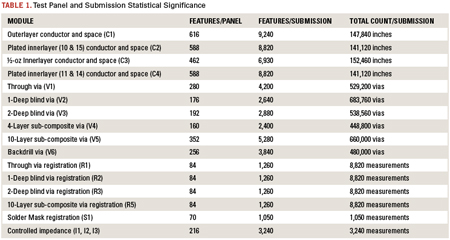
Table 1 highlights the number of features both on this test panel design and the full submission quantity.

Suppliers are expected to complete the 15-panel set in about three months. Third-party testing takes one to two months to complete.
Latest Test Panel Study Results
Some notable observations from our supplier’s most recent test submissions include the following:
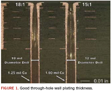
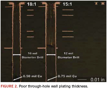
Via daisy-chain defects indicate 0.010" diameter, 18:1 aspect ratio through-hole vias continue to prove to be challenging for some suppliers.2 We found 0.012" diameter, 15:1 aspect ratio through-hole defects are better by a factor of at least three times, but results vary significantly among suppliers. Test panel cross-section photos revealed inadequate hole wall copper plating for both 18:1 and 15:1 aspect ratio through-holes in some cases. Figures 1 and 2 are test panel cross-section examples of good and poor through-hole copper thickness.


Test panels place registration coupons at each corner and amid the central area. Through-hole registration results are provided in terms of percent yields within an allowed radial distance outside a 0.012" drill diameter. Radial distances in this case measure from 0.003" to 0.008" given in 0.001" increments. Test data expectedly show that results are significantly better at the center area of the panel. It may be desirable to consider central panel registration results vs. panel corner results separately, especially in cases when boards are fabricated far from the corners. Combining test results from all areas, the greatest supplier results range for 0.012" through-hole vias was at the 0.006" radial distance.
Thermal cycle testing is performed similarly on all via structures used in the panel design. After test coupons are subjected to six passes of a 260°C assembly simulation reflow profile, they are placed in an air-driven temperature cycling chamber that attains extremes between -40°C and 145°C.3 Next, 4-wire resistance measurements are taken across via daisy-chain structures during cycling. Specifically noted is the number of cycles until 10% resistance change and cycles to open circuit, defined as 20Ω or greater.
Test results show thermal cycle performance does not always correlate to defect density. A supplier may have good defect density results, but poor thermal cycling performance at the same time. Significant differences were demonstrated between the 18:1 and 15:1 aspect ratio vias. 15:1 aspect ratio through-holes attained at least two times the number of thermal cycles achieved by 18:1 aspect ratio vias.
Mechanical blind vias on this test panel are 10-layer, 0.008" and 0.010" drills with aspect ratios of 6:1 and 5:1, respectively. Mechanical buried vias are four-layer, 0.006" and 0.008" drills with aspect ratios of 3:1 and 2.5:1, respectively. All areas of blind and buried via testing, including defects per million vias, registration yields, coefficient of variation, and thermal cycling show significantly higher performance than the through-hole via test results from all suppliers.
Use of lower aspect ratio blind and buried vias combined with sequential lamination and lower through-hole aspect ratios is the preferred build method for ATE boards over the use of high aspect ratio through-hole vias and no sequential lamination cycles.4
One-layer deep microvias utilize 0.003" and 0.004" drills with aspect ratios of approximately 1:1 and 0.75:1, respectively. Two-layer deep microvias utilize 0.007" and 0.008" drills with aspect ratios of approximately 0.85:1 and 0.75:1, respectively. One-layer deep, 0.003" laser drill defect densities continue to be at least two times higher than the 0.004" drill. Supplier results range widely among both drill diameters.
Both two-layer deep microvia drill diameters have significantly better defect densities than the one-layer deep microvias, but supplier ranges still vary widely. There appears a correlation of better results when in-house laser drill is performed vs. outsourced laser drill. Outsourced laser drill is demonstrated to have acceptable results, but considerations in regard to where post-processing and plating is handled should be made, especially if buildup microvia layers are used.
Laser microvia thermal cycling results demonstrate much higher performance than through-hole vias, achieving similar results as the 10-layer mechanical blind vias.
Conductor and space test results are provided for three different layer-types: plated outer layer, plated innerlayer and non-plated 0.5 oz. innerlayer. Plated outer-layers have a surface finish of electroplated NiAu specified at a minimum 200µin nickel underneath 5-15µin gold with Knoop hardness from 130-200. Plated innerlayers are a result of the sequential lamination build in this case and do not have a surface finish.
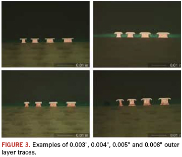
A conductor defect is simply a measurement of an open, and similarly a space defect is measurement of an adjacent short. Conductor defect densities on plated and non-plated inner-layers tended to be acceptably low, with a few supplier excursions seen on the smallest respective widths. Result ranges were observed to be much greater on the outer-layer conductor defects, especially with the smallest 0.003" trace width. Figure 3 shows four different supplier examples of the outer layer 0.003", 0.004", 0.005", and 0.006" conductors. Notably, significant differences are seen among all four examples in terms of copper trace etch factor, NiAu thickness, and length and shape of NiAu overhang.

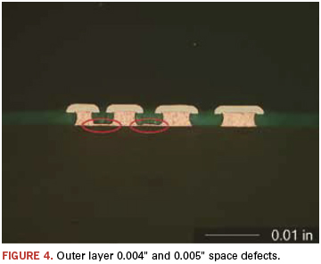
More commonly encountered in ATE board development are space defects, especially when fine pitches are involved, and the test data reflect this. High supplier result ranges are observed on all layer types, especially at the smallest widths tested. Among all suppliers, the highest space defects occur on the plated outer layers. While defects per million inches is substantially highest with the 0.004" spacing and incrementally decreases by whole factors at both 0.005" and 0.006" spacings, very large ranges within supplier results are found on all outer layer space widths. Outer layer space defects were observed on test panel cross-sections (Figure 4).

Managing Test Results Data
After receipt of supplier analysis reports, two applications of the data used are a scoring system and design for manufacturability rules. Developing a scoring system for supplier test panel results is advantageous for many reasons. The number of test results for each individual supplier is extensive. Such a system can be used to simplify data analysis and supplier comparisons. Different scoring weights can be allocated to areas according to the greatest emphases for ATE boards. Ranges for acceptable high and low ends of test results should also be included. Scores are used to identify weak areas and promote competition among suppliers without revealing one’s specific test results to another. Board fabricators can be told non-subjectively where they placed among the supplier base.
Allocating Weights
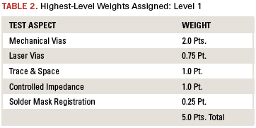
Level 1: The scoring system developed here is based on a 0 to 5 point overall scale. Many different test panel features, feature sizes, and test types require approaching the results on different levels. Level 1 represents the five highest test areas examined on this panel design: mechanical vias, laser vias, trace and space, controlled impedance and soldermask registration.
Based on the 5-point maximum, each area is allocated the weights shown in Table 2. Mechanically drilled vias are understood to be the weakest link in a high-performance ATE board and receive 40% of the total points. Trace and space and controlled impedance each get 20%, laser vias 15%, and soldermask registration 5%. Historically, soldermask registration capability has not strongly impacted ATE board development, but will likely become more important as component densities continue to increase.

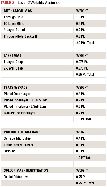
Level 2: Level 2 separates these five areas into their specific feature types. For example, mechanically-drilled vias comprise four different structures on this test panel design: through-holes, backdrill through-holes, 10-layer blind and 4-layer buried. Considerations for the amount of weight to apply to each feature type can include Difficulty to Produce, Frequency of Use, Susceptibility to Failure, and Supply Chain Availability. Table 3 is a breakdown of the five high-level test areas in terms of their feature types and shows the allocated weights assigned to each.

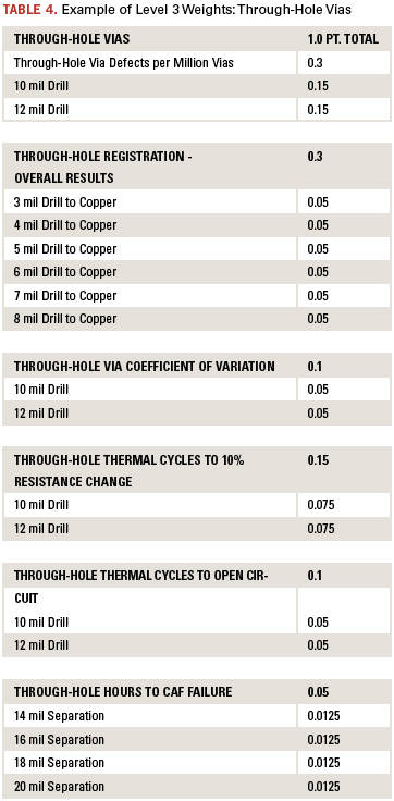
Level 3: Level 3 is the final level and involves specific test panel results. Feature types are further separated in Level 3 by two factors: Type of Test Performed and Feature Size. Six test types are considered for the through-hole vias: defects per million vias, registration, coefficient of variation, thermal cycles to 10% resistance change, thermal cycles to open circuit, and hours to CAF failure.
Considering the two through-hole drill sizes used, 0.010" and 0.012", 18 total test results are applied here for the through-hole feature type. Table 4 is an example of the Level 3 weights assigned for the through-hole via feature type. As with Level 1 and Level 2, weight allocations for specific test types and feature sizes can be based on several factors. In this example, the test types of defect density and registration are each allocated 30% of the total weight, thermal cycling 25%, process variation 10%, and CAF 5%.

All different feature sizes have their allocated weights split evenly in this example, but that does not have to be the case. Emphasis may be placed on feature sizes more difficult to produce or perhaps feature sizes most commonly used.
After weights are assigned to all individual tests, acceptable test result ranges are indicated and used to determine the supplier’s score on a specific test. A supplier’s result is compared against the acceptable range, and then a weight factor is determined. The weight factor is based on where the test result falls within the acceptable range.
Table 5 is an example of the 0.002" radial distance microvia registration for the one-layer deep feature. Here, five supplier test results are shown as A-E. The allocated weight for this test is 0.01875 points, and the specified acceptable range is 60% to 100% yield. In this case, the target is a maximum 100% yield. If a supplier achieves the target result or better, the entirety of the allocated weight is awarded. If the test result is at the farthest end of the specified range or worse, the supplier receives no score. When the result falls somewhere within the acceptable range, the supplier receives a percentage of the allocated weight determined by position within the range. In the example, a test result of 70% yield would earn 0.25 times the allocated weight; 80% yield would earn half, and 90% yield would earn 0.75 times the allocated weight.

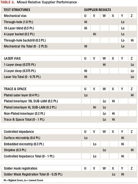
This scoring system is applied to a total of 212 test results for each supplier. Table 6 depicts highest and lowest scores achieved at Level 2 for six suppliers using color coding. Ranges between high and low scores are appreciable in all cases. The table demonstrates that no single supplier exceeds nor fails in all test aspects.

ATE Board DfM
Supplier test results can also be used as the basis for a DfM rule-set. When a multi-supplier strategy is incorporated, test results can certainly be used to determine recommended suppliers based on specific board build requirements. DfM rules should be implemented globally however. This ensures board designs are not limited to single-source manufacturability or perhaps a very limited number of suppliers. Whenever possible, the same aspect should apply such that novel, single-source technology capabilities are avoided if at all possible. DfM minimum and maximum constraints are used to establish quantified limits for improving fabrication yields. Whenever a design allows, absolute minimums and maximums should always be avoided and the number of their occurrences limited.
Mechanically drilled vias with high aspect ratios. As noted earlier, mechanically drilled vias with high aspect ratios have implications that go well beyond a supplier’s ability to merely produce them. This is considered to be the most critical DfM rule to be specified for ATE boards.5 Prohibition of techniques such as flip-drilling, used to attain very high aspect ratio vias, might also be considered. Regardless of how well a supplier can demonstrate the ability of such a process, the result is still a very high aspect ratio via requiring sufficient plating thickness.
Maximum laser drill microvia aspect ratio. Most suppliers specify a capability range between 0.7:1 and 1:1, with 1:1 commonly identified as “engineering level”.
Prohibit mechanical depth drilling for plated vias. The technique of creating blind vias without drilling entirely through a board has proven to yield very poor results in terms of defect density, process variation, and thermal cycling.
Mechanical drill hole wall to hole wall spacing. Drill wander, material properties, wicking, and susceptibility to CAF failure are some considerations in determining this specification.
Mechanical drill hole wall to copper feature spacing. This specification should vary depending on the depth of drilling involved. Test panel registration results provide a good basis for this.
Laser drill hole wall to copper feature spacing. Test results indicate a significantly smaller spacing is feasible among most suppliers than with minimum mechanical drill hole wall to copper feature spacing.
Copper feature to copper feature spacing. Fabricators may indicate this capability as a general minimum to be applied within an entire board, but supplier test results indicate consideration may be necessary for different cases of plated outer layer, plated innerlayer, and non-plated innerlayer.
Supplier Improvement Trends
After test panel data is received, supplier debriefs completed, and improvement plans are communicated, a common question is, Are the board fabrication suppliers getting better? Charts of average defect density trends for through-hole, blind, buried, and laser microvias all indicate supplier improvements. The following graphs represent our specific supplier test panel submissions. It should be noted they are not a representation of the entire PCQR2 database and all suppliers that participated within it.
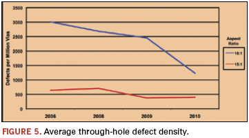
Figure 5 shows that average supplier 18:1 aspect ratio through-hole DpMV has decreased since 2006 from a high of 3,009 to 1,234 from the latest test submissions. Average 15:1 aspect ratio through-hole DpMV ranged from highs of 643 and 708 in 2006 and 2008, respectively, to lows of 375 and 402 DpMV in 2009 and 2010, respectively.

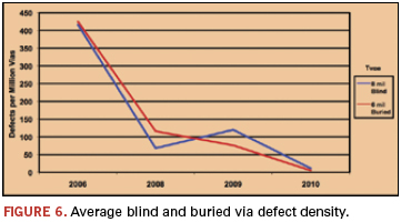
Figure 6 shows 10-layer, 0.008" blind vias had an average supplier defect density of 416 DpMV in 2006. This decreased to 11 DpMV by 2010. For four-layer PCBs with 0.006” buried vias, the average supplier defect density was 425 DpMV in 2006, decreasing to 5 DpMV by 2010.

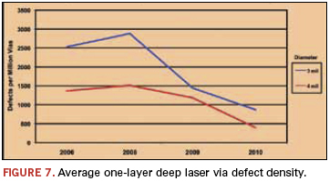
Finally, 0.003", one-layer deep microvia DpMV fell from a supplier average peak of 2,882 in 2008 to 867 DpMV in 2010 (Figure 7). And 0.004", one-layer deep microvia DpMV fell from an average peak of 1,512 in 2008 to 395 in 2010.

Conclusions
Benchmarking and qualifying PCB fabricators for semiconductor test boards requires a quantitative, statistically significant approach that otherwise invites unacceptable risk. Standardized test panels provide a sound basis for engaging with the supplier base and participating in continuous improvement plans. Over time, test panel results objectively demonstrate if suppliers are attaining agreed-upon goals. Since the test panels are close representations of the end-product, it is reasonable that measured process capability, quality and reliability improvements directly impact the fabrication of our ATE platform boards, contributing to maximum entitlement of semiconductor device manufacturing.
Acknowledgments
The author would like to acknowledge the support of Texas Instruments in this ongoing effort, and thank you to Mike Korson in particular. Thanks also to Norm Armendariz, John Hite, Pete Profilet, Martin Gao, Stan Ferrell, Jim Oborny and Marc Mydill. The author would like to acknowledge and thank the support of David Wolf and Tim Estes of Conductor Analysis Technologies. Special thanks to the IPC PCQR2 Database D-36 Subcommittee and all Texas Instruments’ ATE platform board fabricators.
References
1. D.L. Wolf, “Via Reliability – A Holistic Process Approach,” SMTA International, October 2009.
2. Bill Mack, “Benchmarking Printed Circuit Board Fabrication Suppliers Using IPC’s PCQR2 Database,” Burn-in & Test Socket Workshop Proceedings, March 2007.
3. IPC-9151C, “Printed Board Process Capability, Quality, and Relative Reliability (PCQR2) Benchmark Test Standard and Database,” May 2010.
4. Kevin T. Knadle and Virendra R. Jadhav, “Proof is in the PTH – Assuring Via Reliability from Chip Carriers to Thick Printed Wiring Boards,” Electronic Components and Technology Conference, June 2005.
5. Kevin Knadle, “Reliability and Failure Mechanisms of Laminate Substrates in a Pb-free World,” IPC Apex Expo, March 2009.
Ed.: This paper was first presented at SMTA International in October 2011 and is reprinted here with permission of the author.
William J. Mack is test hardware development engineer at Texas Instruments Inc. (ti.com); This email address is being protected from spambots. You need JavaScript enabled to view it..


