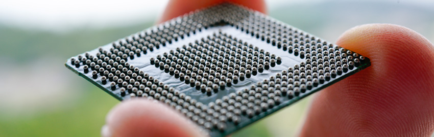
Wherever there is a strong need for improved electrical performance, space reduction, EMI reduction or reliability improvement, utilization of embedded passives will be found.
The foundation of embedded capacitance in printed circuit boards (PCBs) started in the late 1960s. In U.S. Patent No. 3,519,959, the concept of embedded distributed capacitance (closely-spaced power and ground planes for power supply decoupling) was disclosed. In the patent, two layers of embedded distributed capacitance were used. Each embedded distributed capacitor utilized 0.0025-inch thick epoxy glass and two-ounce (0.0025 inch) copper. The use of even thinner and higher performance embedded distributed capacitance material is disclosed in U.S. Patent No. 4,560,962, filed in 1983. In this case, one-ounce (0.0014 inch) power and ground planes separated by epoxy-glass dielectric as thin as 0.001 inch is disclosed. Both these patents are expired, and the teachings disclosed in them, such as the concept of embedded distributed capacitance, are now public domain and able to be practiced broadly. Many OEM designers and PCB fabricators had no awareness of the prior art in the area of embedded distributed capacitance and had a poor understanding of patents. The combination of these two items was a significant impediment to the use of high-performance embedded capacitor laminates prior to 2004.
The interest in embedded passives, especially embedded capacitance, took off in the 1990s. High-speed digital products, with large numbers of ICs switching simultaneously, were seeing a combination of noise and EMI issues due to much faster rise times and lower operating voltages. Portable consumer products, such as cell phones, digital still cameras and camcorders, needed to reduce size and weight while still meeting EMI requirements. Many military/aerospace products had the combination of high performance requirements required by high-speed digital products and the same space and weight constraints seen in portable products. Since the drivers for military/aerospace products were not cost driven, it is easy to see why military/aerospace products were some of the early adopters of the high-performance embedded capacitor (and resistor) technology.
Some of this early interest resulted in an approved DARPA proposal by 3M in 1996. The goal was extremely high-capacitance densities, which could be used in PCBs and MCMs in military products. Both thin-film metal oxides and ceramic-filled polymers were studied over a four-year period. However, it became apparent that ceramic-filled resins, especially barium titanate–filled epoxies, offered the best combination of performance, reliability and PCB fabrication compatibility, as well as the quickest path to commercialization.
At this same time, StorageTek was trying to organize an industry consortium of material suppliers, PCB fabricators and OEMs to study high-performance embedded distributed capacitance materials. The consortia would mitigate the technical resources and funding required to study embedded capacitance in detail. This resulted in the NCMS Embedded Decoupling Capacitance (EDC) consortia. Five embedded capacitor materials, including the 3M embedded capacitor material, were investigated as power-ground cores in multilayer rigid boards. One goal was to confirm that embedded capacitor materials were compatible with all facets of PCB manufacturing, including design, fabrication and reliability testing. Another goal was to determine if the embedded capacitor materials would provide better electrical performance than surface-mounted capacitors, and if so, by how much.
The results were presented to the industry in a final report issued in 20001. It showed that most embedded capacitor materials were compatible with standard PCB processing, had similar reliability results to existing commercial thin, high Tg FR-4 laminates and required very minimal changes in the OEM design or in panelization of the design at the PCB fabricator. Ultra-thin materials (4 µm to 8 µm) with a high Dk were shown to provide excellent electrical performance, much better than surface-mount capacitors or the commercial 2-mil FR-4 material that was being used as a baseline (FIGURE 1 and FIGURE 2).
The consortia provided the initial performance and reliability data that significantly increased the interest in high-performance embedded distributed capacitor laminates and paved the way for a larger follow-up industry consortia on embedded passives. The NIST Advanced Embedded Passives Technology (AEPT) program started in 1999, and the scope of this project was both embedded resistor and capacitor materials, including capacitor functions beyond decoupling.
The NIST AEPT program looked at compatibility of embedded resistor and capacitor materials with non-standard (at that time) PCB fabrication processes, such as laser drilling. Some of these materials were found to be easily laser drilled and compatible with the microvia metallization process (FIGURE 3).
Another important part of the program was to ensure that high-performance embedded capacitor materials could receive UL recognition at the desired levels.
At the end of the program, all three OEMs involved built product emulators with the 3M embedded capacitor material. The product emulators from Nortel, Compaq and Delphi were 10-Gb optical transceiver modules, a PDA and an engine control module (ECM) respectively. All three product emulators were successfully produced by PCB fabricators in the consortia. They were found to be fully functional when tested at the system level, even though a large number of discrete decoupling and/or filter capacitors had been removed from the board surface. The Nortel transceiver module, Compaq PDA and Delphi engine control module (ECM) board are shown in FIGURES 4, 5 and 6, respectively.
In the case of the Nortel transceiver module, the use of embedded capacitance (and resistance) was responsible for reducing the number of layers from 18 to 14, while improving signal integrity by 20%. In the case of Compaq, 74 discrete capacitors were removed from the board surface, while still improving electrical performance. In the case of Delphi, it was shown that an on-engine ceramic module could successfully be replaced by an organic module with embedded capacitors (and resistors). Results were released in a final report to the industry in 2003, and presented in an industry seminar that same year.2
Limited Fab Experience and Supply Base
By 2004, the electrical performance, PCB fabrication compatibility and reliability work done by OEMs such as StorageTek, Nortel, Delphi, Compaq, Sun, H.P. and UL had confirmed the expected electrical performance results on active designs, proven that large number of discrete capacitors could be successfully removed from the board allowing large space reduction and that embedded capacitor laminates had excellent long-term reliability. Also in 2004, the publication of a Printed Circuit Design & Manufacturing magazine article, “The History of Embedded Distributed Capacitance”, greatly increased the industry’s knowledge in the area.3 The combination had mitigated most of the industry’s concerns regarding embedded capacitor laminate materials. However, at the start of 2004, the overall experience of PCB fabricators, especially outside of North America, was very limited. At this time, only 28 fabricators had any experience processing the 3M material. Approximately 25% gained knowledge from participation in the NCMS EDC and NIST AEPT consortia. Of the 28, only nine were from outside of North America, with six from Asia and three from Europe.
By the end of 2008, the number of board fabricators who had successfully processed the 3M material was approximately 100, with approximately 40% of these being in Asia, 40% in North America and 20% in Europe (FIGURE 7).
Lack of Physical Layout and Simulation/Modeling Software
Initially, the lack of physical layout and simulation/modeling software was not a large barrier for embedded capacitor materials because most applications utilized only embedded distributed capacitance. The physical layout was straightforward, replacing the existing thick, low Dk dielectric power and ground planes with very thin, high Dk dielectric power and ground planes of the same design.
If there was a need to determine how many decoupling capacitors could be removed with the use of embedded distributed capacitance, the typical route was to fully assemble the embedded capacitance board and start removing capacitors until you were happy with the performance and the number of caps removed. This process was fine for implementing embedded capacitance on existing designs, the standard practice when initially investigating the technology. However, as designers desired to implement embedded capacitance on next-generation designs, there was a need for simulation/modeling tools to determine power integrity and how many decoupling capacitors would be needed, as designers did not want to design in unnecessary SMT pads, traces and vias.
The very limited software tools available to designers for embedded passives were identified as a large gap early in the NIST AEPT program.4 Even though a few software providers were involved in the program, not much progress was made during its course. The EDA providers did not want to invest a large amount of resources and funding into the creation of software to support embedded passives until there was a known market. This created a chicken-or-the-egg scenario because designers needed the EDA tools to scale up to large volumes.
In the course of the NIST AEPT consortia, much of the physical layout of the singulated embedded passives was done manually. Fortunately, as the use of embedded passives has increased over the last five years, so has the number of available EDA providers and software tools. Today, there are a number of both physical layout and simulation/modeling software tools available.
Improved Discrete Caps and Cost Concerns
Cost concerns are almost always a major hurdle in new technology commercialization, and embedded passives were no exception. From 1998 to 2001, the cost of embedded capacitor bare boards was much higher than the cost of boards without embedded capacitors, due to low volumes, low yields at the embedded capacitor material suppliers and lower yields on embedded capacitor boards during PCB fabrication. This was expected, as the technology was new and very few board fabricators had experience handling thin flexible materials.
Even though embedded capacitance was initially a significant cost adder, the products that really needed it, such as military/aerospace and high-end telecom/computing equipment, could afford the technology. As a result, many OEMs went forward with qualifying the technology. Just as some of the telecom OEMs were ready to implement embedded capacitance into their designs, the telecom bust occurred. Programs slated to use embedded capacitance were either scrapped or went forward with less expensive standard technology.
Also, the discrete component manufacturers were not sitting idle. They could see that embedded passives were a serious threat and continued to not only decrease the costs of discrete components, but also package much more capacitance into the same volume. Additionally, they were able to fabricate smaller components to facilitate designers’ space requirements.
By 2003, a large percentage of the embedded capacitance market was no longer available due to cost pressures. Embedded passive material suppliers needed to improve their productivity and yields to become more competitive. The yields of embedded capacitance boards at the PCB fabricator also had to be comparable to standard product, while market segments beyond military/aerospace, telecom and high-end computing had to be investigated.
During this time, the telecom and high-end computing market showed signs of life and once again began to use high-performance embedded capacitance materials in their rigid multilayer boards. However, only the higher-end products could typically justify the higher increased costs of embedded capacitance technology. These same companies also started investigating embedded passives for high performance chip packages as well. The use of high-performance embedded capacitance materials significantly increased in military/aerospace products, including backplanes and modules, and other market segments, such as medical, began to use these materials in higher volumes.
The use of high-performance embedded capacitance has continued to increase year-over-year. By 2008, it was being used or scaled up in moderate- to high-volumes in essentially every market segment because its high capacitance density is a good fit for use in small modules.
Summary
It has been a very long time coming, but high-performance embedded passive materials have finally hit the mainstream. Designers across the globe have specified it for use, and PCB fabricators in at least 14 different countries have successfully used the material. It has been or is being used in backplanes, rigid, flex, rigid-flex, modules and chip packages. Wherever there is a strong need for improved electrical performance, space reduction, EMI reduction or reliability improvement, utilization of embedded passives will be found.
A recent survey conducted by Printed Circuit Design & Manufacture5 indicated that 11.1% of responders utilized embedded passive technology. The study also found that by 2008, 24.6% of the responders indicated they planned on utilizing embedded passive technology in their designs. Having worked on embedded passives since 1996 and lived through the slow, painful growth of the technology, I feel proud to have been a part of the development, commercialization and scale-up of high-performance embedded passives technology. However, if it weren’t for OEMs such as Compaq, Delphi, H.P., Nortel, Sun and StorageTek; PCB fabricators such as Litton Interconnect and Merix; and material suppliers such as DuPont, MacDermid and 3M, it would have taken considerably longer.
References
1. Embedded Decoupling Capacitance (EDC) Project Final Report, December, 2000. National Center for Manufacturing Sciences, Ann Arbor, Michigan 2. Nortel Presentation, NIST Advanced Embedded Passives Technology (AEPT) Industry Seminar, January, 2003. 3. Joel S. Peiffer, “The History of Embedded Distributed Capacitance,” Printed Circuit Design & Manufacture, August 2004. 4. Advanced Embedded Passives Technology (AEPT) Program Report, September, 2003. National Center for Manufacturing Sciences, Ann Arbor, Michigan. 5. Mike Buetow, “2007: The Year of HDI?”, Printed Circuit Design & Manufacture, January 2007
Joel S. Peiffer is an advanced engineering specialist with 3M Electronic Solutions Division; This email address is being protected from spambots. You need JavaScript enabled to view it..
Connector technology still grapples with smaller platforms, higher speeds and placement issues.
There are thousands of application-specific electronic connector products, with pin counts numbering from one to thousands. Connector varieties mirror the huge diversity of electronics products and applications. Connectors are also used in electrical applications, such as automotive and appliance, and where electronic power connections are required.
A few types of electronic connectors include:
terminals and splices rectangular and circular connectors (including RF/coax) IC sockets connectors for electronic systems (production) connectors for IC test, burn-in and other test printed circuit connectors I/O connectors wire and cable connectors fiber-optic connectors and associated hardware many, many application-specific connector designs
Table 1 breaks out electronic connectors by equipment type. Transportation (automotive electronics and commercial transportation) is the leading user, accounting for 30%, followed closely by information technology (26%), which includes PCs, servers, storage, networks, I/O equipment and point-of-service equipment.
Connectors can be made from a range of technologies, adopting a multitude of new materials and processes, as well as value-added properties such as embedded silicon (memory cards), signal conditioning components (filter connectors), and printed circuits (card edge, FEC – in short, anywhere circuit elements need to be connected).
General use of connectors will not change until PCBs become more integrated. As with other electronics components, connector technology is driven by higher frequency signals, increased packaging densities, assembly processes, industry standards and environmental regulations. Some of the key areas where challenges are expected to occur are described below:
Sub-miniaturization of electronics packaging platform (e.g., HDI, 3-D, printed electronics). Requirements below 200 mm pitch and 0.5 mm mated height may require prototype/experimental interconnect technologies, such as etched foil or MEMS-type micro machining, which would also require some form of micro-robotic insertion. For vertically integrated OEMs, this would have been possible, but is less likely with today’s pervasive outsourcing. Mainstream merchant PCB technology – an area where suppliers tend to have low R&D budgets – is moving in this direction with high-density interconnect (HDI) and microvia technology. Flexible etched circuitry comes closest to the boundary where subminiature connectors are approaching limits. This is primarily in small handheld portable applications such as cellphones, digital cameras, etc. Connector technology continually adapts to new circuit and packaging requirements, and future technologies are expected to enable smaller, subminiature connectors with very thin sections, tighter tolerances and higher temperatures.
Very high-speed interfaces. Serial circuitry and advanced signal conditioning have upped the ante to 10 Gb and beyond. Differential signaling and air dielectric backplane systems have increased copper connectors’ reach to 20 Gbps and beyond. Fiber optics, essentially a point-to-point technology, is a viable alternative (with architectural modifications), as are hybrid Cu-FO designs, which are already in limited use.
Materials cost inflation. Materials cost was a serious issue for connectors and other products in 2006-2007, when copper, nickel, tin gold and many plastic materials experienced major price escalation. Except for precious metals and some other materials, global pricing deflation has occurred with the current recession. Proprietary efforts have had some success in developing minimalist/substitute materials and processes. Connector costs have bottomed, with many units already being assembled in Asia. Time will tell whether the global materials supply chain will help contain costs or contribute to rising prices.
Wireless interconnect. A multitude of wireless technologies are on the market. Some, such as Bluetooth and the recently released Certified Wireless USB, attempt to reduce cable clutter. This will shift some applications into the wireless realm, replacing some connectors. The net effect, however, will be more system-level product volume and, overall, more connector volume. Even in so-called wireless applications, connectors remain.
Potential supply disruptions. Supply-chain risks are associated with a global marketplace, including reduced or eliminated local manufacturing infrastructures as production migrates to Southeast Asia. Many mainstream products are now built in offshore manufacturing venues: notebook and desktop PCs, motherboards, most handheld devices and board-level products for many applications. This dependence on emerging world economies – where there are concerns about infrastructure stability, IP theft, counterfeit products, climate and other issues – could result in supply disruptions. A supply disruption with China, for example, would be catastrophic, and unrest elsewhere could constrict market and EMS manufacturing access.
Use of Connectors with Press-Fit Assembly The Board Assembly chapter of the 2009 iNEMI Roadmap discusses some of the challenges of inserting connectors when using press-fit assembly. Some include:
Automation. Assembly automation continues to be a challenge for some connectors, although the industry has widespread tape-and-reel, tray and other pick-and-place packaging. In addition, odd-shaped component placement has come a long way. However, miniaturization increases the need for higher contact insertion precision. With press-fit assembly, for example, the industry (in some cases) uses slower, manual placement methods to load connectors on the board before the press operation. Manual insertion has become more difficult as pins get smaller, shorter and have higher density, and cycle time for manual placement has increased by an estimated 20%. But even here, some suppliers have designed new press-fit pins.
Currently, there are a limited number of equipment vendors or high-cost robots to automate odd-shaped connector placement onto boards. One reason for the lack of equipment is the lack of standardization of connector trays. Connector manufacturers tend to use trays that match their packaging, and no collaborative industry effort has been undertaken to standardize the trays. Such standardization could go a long way toward being able to automatically place parts for the press operation. Better communication from OEMs and EMS providers to connector vendors would also help. As cost pressures increase, throughput will become more of a focus, and there will be more demand for automatic placement machines, provided they can do some (if not all) of the following steps: pre-optical/laser inspection of pintails, placement, and inspection before the press fit operation. The size of the connector pintail, alignment, true position and average offset of the wafers play a role in the ability to place a connector. AOI use for pintail alignment and true positioning would provide some assurance that connector pins are placed into the holes without stubbing against the PTH wall.
The need for a standard system for automatic pick-and-placement of connectors has been understood for more than 10 years. Different platforms to address this need were released to the market, but due to market conditions, sales were weak and the systems were withdrawn because of demand. Current systems on the market range from semiautomatic presses through fully automatic press systems. However, the automation only pertains to the actual press cycle, while loading the connectors onto the PCB is still manual.
A re-evaluation of the need for a pick-and-place solution is expected with the recovery of the telecommunications and networking industry. The move to smaller pins and denser pin fields is also expected to further drive the need for a pick-and-place option. As the market evolves, one potential solution is to modify an existing automatic press system to act as a pick-and-place or a pick-place-and-press solution. Another potential solution is to take an existing odd-form pick-and-place-system and modify it for use with connectors.
Inspection. Inspection is a critical area of the press operation. Regardless of the type of deformation (accordion, smashed, etc.), the primary concern is a connection that may pass an open/short test, but fail in the field due to the connection opening up. This can occur if the pin shorts to the top of the barrel and passes the electrical test.
If the pins are long enough to protrude through the board, AOI or visual inspection can catch a pin that does not protrude fairly easily. However, if the board is so thick that pins cannot protrude, inspection becomes tougher. Different methods to detect pin presence have been attempted, but no solution works in all situations and is scalable. The feedback system of the press is used at many sites to determine if the press was successful, but even this method is not 100% accurate.
The most difficult and elusive inspection in the press-fit connector process is when two connectors are pressed from both sides of a board, with pins from each connector entering the same hole. There currently is no high-volume algorithm, machine or technique to accurately determine whether both pins are properly inserted into the barrels. As shown in Figure 1, the bottom pin can be bent and still maintain contact with the barrel during assembly and testing. Without a means of accurately identifying that one of the pins is bent, this defect can reach the field and then open up.
Repair. EMS companies are challenged by many different connector types and the rework methods required to remove pins, wafers and connectors. Many assembly sites use pliers to pull the pins, although most connector suppliers sell repair tooling. The need for connector manufacturers to design unique features to permit easy removal, while preventing damage to the PCB, is encouraged, and common tooling to rework connectors is suggested. Connector bodies need to be designed for removing the connector, as well as placing it. Strategically located tooling holes for removal tools need to be designed into the housing. Also, the mechanical strength of the body should be sufficient to permit removal of all pins at once, without mechanical failure of the body.
Key Areas in Development and Commercialization
Connector developments follow OEM requirements, which are now shared with – or referred to – EMS providers. Key areas of interest will include micro and nano materials and process developments, high-speed electrical performance and miniaturization. Mobile/system-in-package (SiP) interconnect requirements may drive future micro-scale robotic connector design plus other dimensional requirements outside the realm of conventional stamp and form/mold connector processes:
BGA attachment with mechanical integrity for advanced SMT applications is now a reality. 10 Gbps now, 20-40 Gbps in the future, with higher-density connectors (> 100 signal contacts per inch), both differential and single-ended signal applications, or low-pin-count serialized interfaces (i.e., backplane systems). High-speed copper and FO cables (Infiniband, Fiber Channel, 10 Gb Ethernet, etc.). LGA socket I/Os have reached 1366 with PC processors; I/Os may drop to 1 or 0.5 mm pitch. New high-performance memory sockets – DDR3, DDRx. Sockets with multi-GHz level signals are dependent on PCB layout; future DIMM may be a two-piece or new design. Serial or parallel optical interconnects; board-level waveguide packaging with optical ICs. Value-added connector assemblies to reduce system cost and complexity, yet sustain the connector function.
Connectors are unique among electronic components because the applications, designs, materials and processes are almost limitless. Many designs have unique customer requirements, while others are multiple sourced industry standard products.
Thus, the industry really has two parts: a huge multi-billion-unit industry or OEM-specific standard segment, and a large semi-to-full customization segment with many market niches and unique customer designs. The roadmap will combine all these diverse characteristics as it seeks to fulfill future industry requirements.
Sidebar
iNEMI Identifies Top Electronics Research Priorities
The 2009 Research Priorities, published by iNEMI, identifies critical areas for research and development over the next 10 years. This document combines findings from the 2009 iNEMI Roadmap with R&D needs identified through an industry-based “gap analysis” process.
The restructuring of the global electronics industry from vertically integrated companies to a complex supply chain dominated by outsourcing has stimulated discussion about how disruptive technologies can effectively be developed and implemented to ensure the continued growth. The iNEMI roadmapping process does not explicitly identify disruptive technologies. It does, however, identify needs – particularly those for which there are no known solutions that meet defined performance and cost requirements. These needs implicitly identify areas for innovation and utilization of disruptive technologies, and they are captured in Priorities.
iNEMI uses Priorities to identify deployment activities in areas where the consortium can have the greatest impact. The information is also shared with iNEMI members, corporate research labs and government funding agencies to help focus R&D efforts for the greatest return.
Another audience for iNEMI Research Priorities is academic research centers. iNEMI distributes the document to leading university-based research centers around the world to help them focus their resources on the areas that are of greatest importance – and relevance – to industry. Academia is playing an increasingly important role in R&D as corporations invest less in long-term basic research. Often, government funding agencies look for industry verification of research topics to help ensure that university funding proposals are relevant to industry needs. Priorities helps university research programs ensure that their efforts are aligned with industry needs.
The document discusses product technology needs for five product sectors: automotive electronics, consumer/portable, medical electronics, netcom systems (networking/datacom/telecom) and office/large business systems. It summarizes research needs within seven categories: manufacturing processes, systems integration, energy, environment, materials and reliability, design, and information management. There is also a discussion of emerging technologies (3-D packaging, printable electronics, energy-efficient technologies and sensors/MEMs).
John MacWilliams is a senior consultant and analyst with Bishop & Associates (bishopinc.com.com) and chaired the Electronic Connector chapter of the 2009 iNEMI Roadmap; This email address is being protected from spambots. You need JavaScript enabled to view it..
Mixing imperial and metric printed circuit board (PCB) design layout units adds a level of complication to the design process. The accepted PCB design process begins with building computer-aided design (CAD) library parts, moves to part placement and ends with via fanout and trace routing challenges. The most basic common denominator in this process is the grid system. Data for machine production can be simplified by using consistent PCB design layout units throughout the design process. In this article, I will review one of the single most important, but basic, aspects of the electronics industry – The PCB design grid system.
From the 1960s through the 1980s, the primary PCB design grid system used Imperial units. All design features and grid layouts were in 0.001-inch (1-ml) increments, and everything was symmetrical and evenly balanced. In the mid 1980s, the International Engineering Consortium (IEC) released IEC 60097 Grid System for Printed Circuits. In 1987, IPC’s SM-782 Land Patterns publication was published with metric dimensions, and in 1988, Congress passed the Omnibus Trade and Competitiveness Act of 1988. This legislation amended the Metric Conversion Act of 1975 and designated the metric system as the preferred system of weights and measures for US trade and commerce. Shortly thereafter, component manufacturers around the globe started using the metric system designations.
The transition from one unit system to another introduced a new level of complication in the PCB design industry because designers were forced to use two different unit systems during the transition period. The complication became even more pronounced with the introduction of gridless and shaped-based autorouting. The main impact of the gridless system for PCB layout is the fact that trace routing computations are so granular that they consume far more memory and central processing units (CPUs). The gridless system has tens of thousands of additional options to commutate and actually slows the autorouting tools down. It also makes it extremely difficult to cleanly route traces in between the center of two component leads or vias manually. The universal PCB design grid system impacts everything from CAD library creation to part placement, from via fanout to trace routing, while consuming far less computer memory and CPU processing. It also centers traces between pins and vias, increasing manufacturing yields while improving the overall aesthetic look of the part placement and the trace routing. The ultimate goal for IPC Standards and for designing a perfect PCB is to have all element feature sizes in the PCB design rounded off in 0.05-mm increments and snapped to a 0.05-mm grid system. The following pages explain the criteria needed to follow this universal PCB design grid system and to learn how advanced it really is.
Land Pattern CAD Library Creation
With guidance provided by the organizations in the accompanying sidebar, PCB designers have built rules for creating consistent, quality land patterns in their CAD tools. In the ideal universal grid system, 0.05 mm matches many elements. There are unique exceptions to these rules, but these are true most of the time.
Generic Sizes for all CAD Library Land Patterns for both SMT and PTH according to IPC:
Outlines are in 0.05-mm increments, includes silkscreen, assembly and placement courtyard. Pad sizes are in 0.05-mm increments. Hole sizes are in 0.05-mm increments. Polarity markings are in 0.05-mm increments. Local fiducials are in 0.05-mm increments. Reference designator height and line widths are in 0.05-mm increments. Ball Grid Array Standards for Packages in the IPC-7351 Standard: Ball and sand sizes are in 0.05-mm increments. Pin pitches are on 0.05-mm increments. Package body outline dimensions are in 0.05-mm increments. Gull Wing Component Lead Standards for QFP, SOP and SOT Packages from JEDEC: Package body outline dimensions are in 0.05-mm increments. Package tolerances are in 0.0-5mm increments. Terminal lead sizes are in 0.05-mm increments. Pin pitches, land size round-offs “X, Y” are on 0.05-mm increments and land centers “C” are on 0.1-mm increments. (See FIGURE 1).
Chip Component Lead Standards for Resistor, Capacitor, Diode and Inductor Packages by EIA:
Package body for outline length and width dimensions are in 0.05-mm increments. Terminal lead sizes are in 0.05-mm increments. Land size round-offs “X, Y” are on 0.05-mm increments & land centers “C” are on 0.1-mm increments. No-Lead Component Lead Standards for SON, QFN, DFN, SOTFL and SODFL by JEDEC: Pin pitches are on 0.05-mm increments. Package body outline dimensions are in 0.05-mm increments (includes height). Terminal lead sizes are in 0.05-mm increments. Package tolerances are in 0.05-mm increments.
The basic rule, in today’s component package technology, is that most of the time component package dimensions and solder terminal leads are in 0.05-mm increments. The exceptions to this rule are all component packages that have been carried over from the 1980s. In order for a complete transition to the metric system and a the introduction of a full-blown electronic product development automation, the inch- based component packages would have to be eliminated.
Part Placement Grid System
If you build your CAD library parts in millimeter units, the best placement grid rule is to use numbers that can be evenly divided into 1 mm and are one place to the right of the decimal point. Optimized metric placement grids include: 1 mm, 0.5 mm, 0.2 mm and 0.1 mm. To achieve the best results, no other part placement grids should be used unless absolutely necessary (for instance, in the case of a fixed connector or switch on the PCB edge).
Via Size and Fanout Grid System
Via padstack sizes are in increments of 0.05 mm. This includes all via hole sizes.
The best via padstack for overall trace routing is: 0.5-mm pad, 0.25-mm hole and 0.7-mm plane antipad.
If every via in the PCB design was placed on a 1-mm grid system, the traces could be routed across the design layout without unnecessary bends. The best via fanout grid is 1 mm. This allows for two 0.1-mm traces to be routed in between vias, as illustrated in FIGURES 2, 3 and 4.
Figure 4 clearly illustrates two vias snapped on a 1-mm grid with two, 0.1-mm traces perfectly centered between them. You can also route one, 0.1-mm trace between the vias perfectly centered. The plane antipad does not encroach under the traces and provides a clean return path on the reference plane. This is a superior routing solution for high-speed technology while providing a simplified working environment.
Trace / Space Size Grid System
Metric trace width rules are in increments of 0.05 mm with one exception: 0.125 mm (5 mils). 0.25 mm = 10 mils 0.20 mm = 8 mils 0.15 mm = 6 mils 0.125 mm = 5 mils 0.10 mm = 4 mils 0.075 mm = 3 mils 0.05 mm = 2 mils
Trace Routing Grid System The ultimate metric routing grid is 0.05 mm.
Reference Designators and Text Grid System
The common grid for placing reference designators and text is 0.1 mm, but 0.05 mm is used for tight spaces. Copper Pour and Plane Fill Grid System
The common grid for copper pour outlines and snap grid is 0.1 mm, but 0.05 mm can be used for high- density part placement and trace routing.
Mounting Hole Size and Placement Grid System
All mounting hole padstacks are in increments of 0.05 mm, and the placement grid is in 0.05-mm increments.
Conclusion
The United States is now the only industrialized country in the world that does not use the metric system as its predominant system of measurement. However, PCB design worldwide has been historically driven by component manufacturers and CAD vendors to use the Imperial measurement system. Clearly, U.S. companies that do not produce products or services to metric specifications will risk becoming increasingly noncompetitive in world markets. Japan has identified the United State’s lack of metric usage as a strategic impediment to access its products to the Japanese home market. In addition, consolidation of the European market product standards will make sales of nonmetric products increasingly difficult and uncertain. Most U.S. companies understand that using metric units is essential to future economic success.
Through their actions, U.S. Federal agencies are demonstrating an increasing determination to use the metric system in business-related activities. For example, most component manufacturers have converted their component dimensional datasheets to millimeter units. Many of the results are not yet visible to the public, which is not a direct target of current Federal transition activities.
Industry acceptance of the metric transition is due partly to the realization that producing to metric specifications and surviving in tomorrow’s economic environment are synonymous. Today, most companies export their products to a global market where metric-based products are expected.
Sidebar
Electronic Standard Organizations
Standard component package outlines come from industry standard organizations that specialize in component packaging data and standardization of documents and publications.
Standards organizations descriptions :
JEDEC – Joint Electron Device Engineering Council. This semiconductor engineering standardization body represents all areas of the electronics industry including discrete component and integrated circuit packaging standards.
EIA –Electronic Industries Alliance. A national trade organization that includes the full spectrum of U.S. manufacturers for tape and reel, tray and tube component packaging standards. The EIA-481-D-2008 publication is the most recent.
IEC – International Electrotechnical Commission. IEC is the leading global organization that prepares and publishes international standards for all electrical, electronic and related technologies, as well as associated general disciplines such as terminology and symbols.
NIST – National Institute of Standards and Technology. From atomic clocks to semiconductors, innumerable products and services rely in some way on NIST. NIST’s mission is to develop and to promote measurement, standards and technology to enhance productivity, to facilitate trade and to improve the quality of life.
IPC – Association Connecting Electronics Industries. IPC is the only trade association that brings together all of the players in this industry: PCB designers, manufacturers, assembly companies, suppliers and original equipment manufacturers (OEMs).
ANSI – The American National Standards Institute. ANSI’s mission is to enhance both the global competitiveness of U.S. business and the quality of life by promoting and facilitating voluntary consensus standards and conformity assessment systems, while safeguarding their integrity.
EIAJ – Electronic Industries Association of Japan. EIAJ’s mission is to represent the domestic electronics industry in working on the challenges and issues it faces including programs planned and implemented with the cooperation of related organizations and associations worldwide.
NEMI – National Electronics Manufacturing Initiative. NEMI is an industry-led consortium whose mission is to assure leadership of the global electronics manufacturing supply chain. It has a membership that includes hundreds of electronic component manufacturers, suppliers, associations, government agencies and universities.
JEITA – Japan Electronics and Information Technology Industries Association. JEITA is an industry organization in Japan with activities covering both the electronics and information technology (IT) fields. JEITA covers electronic components, radio and broadcasting equipment, computers, medical devices, measure and control systems and assemblies.
Tom Hausherr is an EDA library product manager with Valor Computerized Systems. He can be reached at: This email address is being protected from spambots. You need JavaScript enabled to view it..
Surface roughness can originate from a number of sources; imbalances in the organic additives and improper filming of the copper anodes are key contributors.
In this month’s column, the subject of surface roughness and some lesser-known plating anomalies are discussed/examined. In general, surface roughness is often attributed to particulate matter that is not being filtered from the plating solution; however, roughness can also be caused by a number of other factors. A few of these factors are shown below, with a brief discussion of the root cause or causes of the roughness.
In FIGURE 1, the plated circuit trace is excessively roughened. Upon further examination, it is quite clear that the cause of the rough deposit is residues that remained on the surface of the base copper. Perhaps the team should look carefully at all rinsing and filtration steps leading to the electrolytic copper process.
A common anomaly is seen in the form of a raised area in the electrodeposited copper. This, of course, should be considered a rough deposit. At first glance, the operators may assign the cause to a low concentration of the organic addition agent. Typically, when that assumption is made, the reaction is to add more organic addition agent to the plating solution, but that will cause additional harm to the functioning of the plating solution.
On occasion, one gets a call from a frantic PCB fabricator describing a situation one could call “stringy nodules” or “hairs” as seen in FIGURE 2. Obviously, without first seeing the actual defect, the image that this conjures up can bring about a long brainstorming session as to the root cause of the anomaly.
These stringy nodules have their origin, usually in one of three areas:
organic contamination in the copper plating solution
improper brightener and carrier concentrations
improperly filmed anodes.
It is unlikely that particulate matter floating around in the plating solution causes these stringy nodules, unless the copper anodes are not filmed up properly. In other words, the success of acid copper plating depends in part on the uniform corrosion of the anodes during electrodeposition. In order to insure this, the uniform black film must be present on the anodes, and this film should not be disturbed once it is formed. If the film is not forming properly, one may expect to see these types of nodules, as well as issues related to excessive consumption of the organic addition agents (brighteners, etc.). This will cause the various components of the additives to be out of balance, which will lead to plating anomalies such as stringy nodules and roughness.
A summary of the causes of the various plating anomalies presented in this article is:
Debris
poor anode quality
poor filtration
ASF too low or high
particulate material on substrate prior to entering bath and/or in bath
Residues / Cleaning Issues
poor upstream processing
weak pre-cleaning
strings
organic contamination
improper brightener and carrier concentrations
improperly filmed anodes.
Remember, surface roughness can originate from a number of sources, including organic additive imbalances and improper filming of the copper anodes. Certainly, good troubleshooting starts with a thorough investigation of the plated surfaces, the pre-plate conditions and the potential for particulate matter that, for some reason, is not removed by filtration.
Michael Carano is global manager for strategic business development at OM Group, Inc. and can be reached at This email address is being protected from spambots. You need JavaScript enabled to view it..
The best surface finish meets the needs of the board design and the assembly process, while being easy on the wallet.
Selecting the right final finish should not be a puzzle, but it can seem like one. Often, there is conflicting information about different finishes and their intended applications. Depending on one’s point of view, bias enters into the equation, and sometimes, conclusions can be reached that outweigh the data. The best surface finish meets the needs of the board design and the assembly process, while being easy on the wallet.
From a fabrication house perspective, the ideal surface finish is: inexpensive to apply and to stock (think pounds of gold or tons of solder); easy to set up, control, maintain and run; reworkable; and operational with little experience.
If you are a contract manufacturer, your focus and needs are a little different. You might be looking for a surface finish that provides good-looking solder joints (regardless of the assembly materials or the process used), is easy to rework, can sit in process for as much time as needed without fear of future problems and has a long shelf life. The OEM, on the other hand, is most interested in cost, reliability and availability. Chemical vendors may have a very narrow point of view highlighting the advantages of their latest system at the expense of all other surface finish options. When you couple all these different points of view with some personal experiences (set in time) and bias, the resulting confusion can be understandable.
Hot air solder level (HASL) came into the industry to replace fused, tin-lead solder. By using solder mask over bare copper (SMOBC), a fabricator could easily protect base copper and have a solderable surface finish. HASL was introduced just prior to the advent of SMT. We should give credit to the equipment manufacturers and engineers who found a way to improve air knife geometries and fluid dynamics, keeping this a viable option for the last two decades. Solder-coated copper has taken much of the work out of soldering at the assembly house because the tin-copper inter-metallic layer is already formed. The heat required at assembly is just enough to fuse HASL solder with solder paste. HASL boards have excellent shelf life and are easy to rework at both fabrication and assembly. If properly assembled and cleaned, they will have very little field failure concerns that are more common with other finishes.
However, HASL does not lend itself well to high-density boards. Once SMT pitch goes below 16 mils or pad co-planarity is an absolute requirement, HASL will not perform well. Solder thickness can vary between 35 micro inches to 1500 micro inches. Lead-free solders have higher surface tension then standard 63/37, so pad planarity will be better, but pad wetting will suffer. Small, solder mask-defined features will be difficult to wet with one pass. One major issue with lead-free HASL is copper dissolution. If standard SAC 305 is used, expect to have more copper plate required to overcome what will be lost in the solder pot, typically 20% to 30% more then standard. Proprietary, lead-free solders consume much less copper, so less copper plating is required. HASL can be applied with vertical or horizontal equipment, providing better pad wetting and flatter pads – but the cost of equipment can easily outweigh the benefits. Shelf life is typically 12 months from the date of application. Although HASL is readily available, some US companies have removed their equipment, opting to subcontract this process.
Organic solderability preservatives (OSPs) have also evolved from simple anti-oxidants to thicker, more thermally stable coatings able to withstand multiple, lead-free reflow cycles (FIGURE 1). OSPs cost the least to purchase and to operate but, perhaps, place more burden on the assembly house. The OSP coatings are commonly available on the market, ranging in thickness between 0.10 microns and 0.50 microns. Ideally suited for SMT applications, they also produce excellent solder joint strength. Handheld devices commonly use a combination of electroless nickel/immersion gold (ENIG) for key contact areas with OSP on soldered pads because the solder joint strength is superior and will stand up to multiple shocks. OSP can be found on the simplest of designs, for companies with the lowest expectations for reliability, to the most difficult designs, from OEMs that require absolute confidence for products with 10-year to 20-year life cycles. OSP is an insulator, making it unsuitable for key contacts and difficult for in-circuit testers. It requires fluxes that are active enough to dissolve it before solder can react with copper. Flux must be applied directly to the OSP in order for solder joints to form. If solder paste is applied to the board, any area the paste contacts will remove the OSP, so rework and assembly must begin right away. Once applied, the coating’s shelf life ranges from 6 months to 12 months, depending on the supplier’s recommendations. OSPs can run vertically or horizontally, and the cost of equipment is low. They are available from many board fabricators, and the surface finish covers nearly 40% of PCBs that are produced today.
Immersion tin (ISn) has been in the industry for quite some time. Early bath versions were simple and cheap to operate but provided questionable solderability and were prone to generating tin whiskers. Modern baths perform much better and have whiskering under control, due to the incorporation of better coating morphology and anti-whiskering agents. Immersion tin baths are hot and acidic, requiring careful soldermask surface preparation and tight soldermask process control in order to survive the tin-plating bath. Immersion tin is favored by the automotive industry and is a particular favorite for press fit applications. It has shown excellent color stability throughout assembly product life and has proven to be effective in harsh environments. In-circuit testing is not an issue because the coating is conductive. It can be run vertically or horizontally, but unless production needs are high, vertical equipment is most desirable. While immersion tin is widely used, not all board shops have the process installed.
The ENIG process came into play in the early 1990s as a coplanar surface finish to replace HASL. Early on, issues with bath stability, skip plating and extraneous plating required very tight process controls and process development. Later, black pad became an issue. In large part, these issues have been overcome, but black pad still seems to come into play on occasion. This particular problem stems from the chemical attack of the nickel layer, resulting in inconsistent or questionable solder joint strength. An automatically controlled vertical line, with properly controlled baths from a reputable supplier, should not suffer from this issue. ENIG has many benefits including excellent shelf life, easy rework at assembly (but not at the board house), low contact resistance, excellent solderability and good solder spread. The downsides include cost of operation, soldermask attack, high demand for shop utilities and a tight process window. ENIG is the most expensive surface finish to apply because pricing is tied to gold values and thickness. All that being said, ENIG usage has risen dramatically over the past few years, and it is widely available in the industry (FIGURE 2).
Electroless nickel, electroless palladium, immersion gold (ENEPIG) has recently started to be used in the PCB industry, with the promise of being a universal finish. A universal finish is solderable, can be used for key contacts, edge rails and mating surfaces and is wire bondable. It has all the benefits of ENIG but eliminates the black pad phenomena by eliminating the potential for gold corrosion of the nickel. Like ENIG, ENEPIG also adds the benefit of a nickel barrier over the copper, eliminating any potential for copper dilution issues that have been seen with other surface finishes. However, it operates at a high cost, will attack soldermask and is relatively new to the industry, so failure modes have not been fully characterized.
Immersion silver (IAg) is the most cost-effective, metal, surface finish alternative to HASL (FIGURE 3). It has excellent soldering characteristics and is highly conductive. Baths are stable, with relatively mild chemistries, and dwell times are quick so it is easy to conveyorize. Although IAg seemed poised to replace HASL as the dominant surface finish, recent industry issues related to performance in harsh environments has exposed a weakness of the coating; creep corrosion. When placed in sulfur-rich environments, silver catalyzes copper sulfide formation that can lead to shorts in the final assembly. Initially, studies placed the blame solely on the immersion silver finish, but recent work has shown assembly materials are perhaps a more significant contributor to the problem. The industry has responded with new immersion silver post treatments that either suppress the corrosion reaction or keep the corrosion localized to unsoldered areas. Immersion silver can be run vertically or horizontally, and equipment costs are low. Most shops have immersion silver installed.
A new option is available to the market that can replace ENIG. Organic metals (FIGURE 4) show excellent solderability, operate at lower temperatures, have shorter dwell times and are highly conductive. They also have lower material costs than ENIG and have reduced requirements for power and water, resulting in a much lower cost of ownership for the fabricator. This type of process will generate a finish that looks closer to an OSP, but with superior hole fill and in-circuit test capabilities. Because they are new to the industry, availability is limited, but demand will force more installations in the near future.
Surface finishes can be puzzling, but with the right information, knowledgeable decisions can be made for the best fit keeping in mind the needs of the board fabricator, assembler and OEM.
Jim Kenny is global product line manager, PWB final finishes, Enthone; This email address is being protected from spambots. You need JavaScript enabled to view it..
Industry forces enable the highest cutting-edge technology but can end up at odds over the day-to-day minutia of business.
It’s amazing the amount of creativity our industry has. Designers can take conceptual ideas and develop designs that, when combined with various components, turn those ideas into reality. I appreciate designers because they make product development look easy, as they think through what is needed vs. what is available.
Fabricators display creativity in a different way. They must understand chemistry, mechanical engineering, software manipulation, additive processes and removal processes, as well as thermal engineering – all the things needed for fabrication. They require creativity to continually move the bar higher, while utilizing equipment and materials that were not necessarily designed to produce the required results.
Material suppliers – chemical, laminate or something in between – are an equally creative bunch. Whether developing new and/or hybrid products, modifying existing materials to handle the reduced line/space, dimensional requirements and higher thermal requirements, or meeting the environmental standards thrust upon them by non-technical bureaucrats in Government, they demonstrate a keen ability to provide raw materials that are needed to produce the level of technology required to be competitive. Such efforts indeed require and demonstrate real creativity.
With so much creativity evident throughout the industry, we have never needed it as much as we do now. All too often, the creative forces that can enable the highest cutting-edge technology end up at odds over the day-to-day minutia of business, resulting in both short- and long-term suffering. When the economy contracts, the pressure is to get orders and squeeze everyone for the best price. This type of squeeze play always reduces true value and mutually beneficial relationships to a level where no one wins and dividing lines get drawn. Many companies experienced some of that a few years ago when the tide toward Asia swept much of the demand for circuit boards away from the western shores. The first thing many did was start to beat up the supply base, seeking lower prices.
The response was to receive somewhat lower pricing at the expense of technical support and real product development, with many suppliers falling by the wayside. Other companies had to make the painful choice to either continue developing new products or providing the same level of technical support. Those who developed products but decreased support could only afford to market to large customers, most of which were in Asia. Those who did not develop product had little to support, and the combined result was an accelerated demise of the industry as we knew it.
Today, our industry in the West is very different than it was a decade ago. Equally, the industry in Asia is experiencing its first global downturn, causing many companies to rethink how they operate. It seems that we have great examples of what happens when we pit ourselves against other links in the supply chain. Maybe we need to step back and rethink how we treat each other– with an eye toward adding value and becoming stronger, more viable companies in a dynamic industry.
Fabricators and suppliers really need to get to know each other better. How can a supplier’s new products help a fabricator achieve higher technology that commands higher prices from more customers? Equally, how can fabricators introduce suppliers to designers who are pushing the envelope? Suppliers need to work with their “un-sales” departments, such as accounting, and remind them that it’s all about long-term relationship, and fabricators need to make their purchasing efforts more proactive for service and technical support – not just price. When the goal is providing value and building a relationship, individual order price and terms should never be the driver.
In addition, fabricators and suppliers need to work together to provide designers with better technical resources so the next, great design can be developed and brought to market with the best available technology in a cost-effective manner. All parties lose when interpersonal technical support and involvement are replaced with flat emails. If there is one aspect of service that our technology-driven industry seems to have forgotten, it’s how to be a solutions provider, working together across the entire supply chain.
Finally, most of the companies who are still in business are technologically competent companies. Customers need and expect technology, and the supply chain at all levels has creative, can-do people who shine when they are given a task that will lead to a new product or radically improved technology. So shouldn’t we all recommit ourselves to making sure that, in this economic downturn, we excel in satisfying our mutual customers’ needs by working together to enhance capability and providing true value to each other – as well as the industry? Maybe we will find that profits can and are earned by everyone in the supply chain when creatively developing the new, rather than by pointing fingers and dwelling on the old.
Peter Bigelow is president and CEO of IMI (www.imipcb.com); This email address is being protected from spambots. You need JavaScript enabled to view it..