Simulation generates a prediction of signal-dependent PDN noise that can be used to predict board-level emissions.
Just as the board design community is becoming familiar with signal integrity, along comes the next hot topic – power integrity. The objective of board-level power integrity (PI) is to assure adequate current is delivered to all mounted devices within a tight voltage margin, as DC power requirements and AC switching activity change dynamically. PI challenges are of growing concern because of several parallel trends. Total power and current requirements are creeping upward, while voltage levels are dropping. With lower voltage comes lower power delivery network (PDN) and signal noise margins. Switching speeds are getting faster and high-speed serial and parallel interconnects are becoming more pervasive.
DC Power Integrity
DC PI design flows begin with static power consumption specs, including voltage and current for each power rail, as well as DC noise margins and IR drop constraints. Detailed board-level DC simulation solutions are readily available and run quickly for even large boards. Constraint-driven EDA solutions are more the norm than the exception. DC PI simulations are typically setup early in the design flow and can be quickly performed as incremental validation checks when board designers update the design. Physical prototypes and measurements, based DC PI design flows, are too time-consuming and not flexible enough to meet modern design challenges.
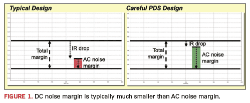
DC noise margins are typically more stringently specified than AC noise margins. It is not atypical to allocate only 20% of the total available PDN noise margin for DC (FIGURE 1). This is possible because their behavior is modeled much more completely than those for AC simulation. This is due to the fact that localized coupling and PDN-global effects, such as resonances, do not exist for DC.
Stackup design is the first task with design controls available for a number of layers and power plane metal thickness. Applying two-ounce copper layers everywhere would help thermal concerns and DC power delivery, but it is unnecessarily expensive and increases overall board thickness and design weight. AC signal routing concerns also drive stackup selection, but only DC simulations are performed to validate choices made at the pre-placement stage in the design flow.
Mounted device placement is the next step, including PDN components such as the voltage regulator module (VRM) and remote sense lines – low current control nets to detect remote voltage levels. Key considerations are high via currents and plane current densities in the region of attachment of the VRM to the PDN. EDA support is available for optimizing sense line placement, which can help recapture significant DC noise margin that otherwise would be wasted.
Vias between planes are an important consideration throughout the entire PDN. They must be placed properly to avoid vias that carry little current, resulting in wasted space and likely current constraint violations. In addition to constraint tables, color-shaded plots are available for both via currents and plane current densities.
AC Power Integrity
Typical AC PI design flows are considered in two distinct stages, each of which is reviewed in detail below. The first stage involves frequency domain analysis and measurement techniques to examine frequency-dependent PDN impedance. Capacitors are selected and placed between the power and the ground nets to provide transient switching currents to mounted devices. This task is performed after device placement on the PCB but prior to routing signal traces because routing changes are difficult to make later in the design flow to accommodate additional capacitor placements local to mounted devices. The second design stage is performed after signal routing and involves detailed analysis of both the PDN and the signal nets to examine transient PDN noise. Driver/receiver electrical models couple transient signals with the associated switching current flow in the PDN. Of particular interest for AC PI is the case of many signals switching at the same time, called simultaneous switching noise (SSN).
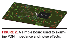
A simple six-layer board design is applied to investigate AC PI effects, as shown in FIGURE 2. The stackup is SGSSPS, where S=signal, G=ground, P=power.
PDN Impedance
Low frequency-dependent impedance between power and ground assures low transient noise voltage when currents are pulled through the PDN to drive switching signals. Target impedances are different for each device and sometimes for different pins within the same device. Not all vendors provide specifications for target impedance, but it is easily approximated based on allowable AC noise margin (ΔV) and power rail switching current amplitude (IAC), as Ztarget = ΔV / IAC. For a 1.5-V power rail with +/-5% total noise margin and 80% allocation to AC noise, ΔV = 60mV. A switching current of 5 A implies target impedance for the power rail of 12 mΩ. Since multiple pins exist for each power or ground net, the per-pin impedance would be larger; however, it does not decrease linearly with pin count because switching current does not flow uniformly in all pins. Board-level target impedance is rarely frequency-independent because switching currents have non-uniform frequency spectra. Further, board PDN impedances are dominated by inductance at high frequency and rely on package and silicon for noise filtering and local decoupling capacitors (decaps) to provide on-chip switching currents above 200 MHz to 500 MHz.
The simple board of Figure 2 is examined to help understand PDN impedance and the physical effects that cause frequency-dependence. The signal nets are ignored and only the power/ground nets are examined. Frequency domain, board-level AC simulation is performed prior to fabrication, although the same impedance is often measured in the lab for physical prototypes using a vector network analyzer (VNA). PDN impedance is most often characterized for bare boards because precise analysis is difficult due to a lack of accurate models for all devices connected between the power and ground nets of the PDN.
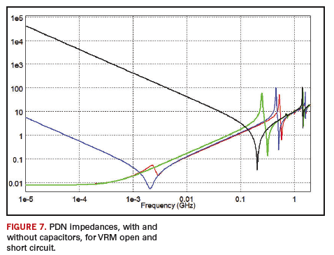
Impedances are characterized looking into the PDN from the location of a mounted device. FIGURE 3 shows the bare board PDN impedance looking into device U17 indicated by a white arrow in Figure 2. An external VRM is connected to the multiple power/ground pins of the card edge connector in the lower/right portion of the board. The black trace is for the VRM open circuit, and the green trace is for the VRM short circuit. The trace is high impedance at low frequency with a slope of -1 on the log-log impedance plot. This represents the capacitance of C=370 pF between the power and ground nets. The green trace, as one expects due to the short circuit at the card edge connector, reflects DC resistance of R=8 mOhm below 250 kHz and loop inductance from the probe to the VRM of L=2.7 nH below 100 MHz.
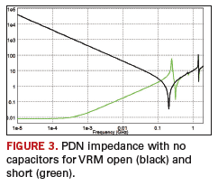
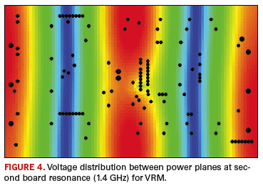
Energy traveling in the board laminate material at 200 MHz has a wavelength of more than 700 mm; therefore, these LC parasitics are lumped circuit effects for this board because the board dimensions are a small fraction of a wavelength. The first dip in the black curve and the first peak in the green curve at 200 MHz are a series LC and a parallel LC resonances. The first plane resonance is where the 100 mm length of the board is a half wavelength, just above 700 MHz. This resonance has a voltage null in the center of the board very near the PDN impedance probe. Therefore, it has little effect on the PDN impedance curves, demonstrating that plane resonances affect various regions of the board in very different manners. The second plane resonance along the length of the board, shown in FIGURE 4, occurs at about 1.4 GHz and has a voltage peak near the probe location. Figure 3 shows the expected large resonance effect at 1.4 GHz. Larger boards have larger-valued L and C parasitics and, therefore, lower frequency lumped resonances. For arbitrarily shaped planes, the resonances are difficult to predict with simple expressions, where the first few resonances were known to be at multiples of a half wavelength along the length of this simple, rectangular board.
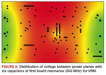
Since plane resonances can dramatically affect PDN impedance, they should be avoided. One way to accomplish this is to add capacitors between power and ground. These capacitors provide switching current and become short circuits at high frequency to eliminate resonances. Six 0.47-nF capacitors are attached to the PDN of the example board – three on each the left and the right side. These are typically called decoupling capacitors (decaps). They add to the lumped C parasitic of the board; therefore, the lumped LC resonances drop to about 200 MHz, as shown in FIGURE 5. At higher frequencies, the capacitors form a low-impedance path between power/ground planes and significantly change plane resonance patterns. Voltage maxima, previously at the left/right edges for the first plane resonance, become voltage minima, with a voltage maximum now near the probe. The loading of the capacitors drops this resonance to about 500 MHz, with a voltage distribution as shown in FIGURE 6.
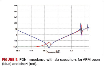
Above the 2-MHz-lumped LC resonance, the impedance becomes inductive (slope of +1). With the addition of six decaps, the effective inductance is reduced because additional low-impedance current paths now exist at the edges of the board through capacitors. This can be seen in FIGURE 7 by comparing the red and green traces above 2 MHz and below the first plane resonances. If more decaps are placed on the board, the resonances are further changed and the high frequency inductance-dominated PDN impedance is further reduced.
This process of adding decaps, examining resonances and then choosing new decap locations and values can become tedious for designs that require more than a handful of decaps. This process is usually simulation-based and implemented in commonly available EDA solutions. Measurement-based flows are rare because physical prototypes require too much time to manufacture, and it is difficult to measure resonance voltage distributions to know where to locate new decoupling capacitors. The effort involved in crafting a low-impedance profile through analytical decap placement and component selection leads many designers to over-design unnecessarily expensive boards with too many decaps. Design rules are applied, such as use one decap per power pin and apply the largest decap available for a given component size. It is rare this many decaps are required and, as demonstrated in the previous example, using a larger-valued decap leads to a lumped resonance frequency that is potentially too low. There are EDA solutions that can optimize board designs for high-performance (low PDN impedance) and low-cost decap schemes. These solutions are applied at the post-placement/pre-route stage, during post-layout verification or even for post-production enhancements.
PDN Noise
Design goal specification and measurement verification of both PDN and signal noise is ultimately a time domain issue for end products. PDN noise is a function of the transient currents pulled by switching circuits to drive signals between logic states. Therefore, PDN noise is dependent on signaling conditions. Lower target impedances should be specified for frequencies with high switching current content. Since signal nets reference the local PDN to define signal voltage, PDN noise results in higher signal noise. If many signals in a region of the board switch at the same time, there can be high switching current flow in the PDN, resulting in high signal noise. In addition, if the signals all switch simultaneously from one logic state to the other, signal net proximity couplings can sum to become larger. This condition is called simultaneous switching noise (SSN) and is of great concern for DDR memory buses and multi-channel, high-speed serial interconnects. SSN is commonly perceived as a signal noise issue, but this simple board example demonstrates it is dominantly a PDN issue.
PDN noise is characterized for the same simple board for which PDN impedance was previously examined. The six decaps added are retained because the PDN impedance is lower with them present. The same PDN probe location is applied, only now, transient simulation or an oscilloscope are applied to characterize the PDN in the time domain. IBIS drivers are specified for the 16 single-ended signal nets with signal sources at the mounted device U17 on the top of the board. Eight resistive terminations are applied at each of two separate memory devices on the board. The signals are routed on a combination of the four signal layers, with the bulk of the routing occurring on the bottom microstrip and two middle stripline signal layers. As recommended for SSN simulations or measurements, one signal is tied high, one is tied low and the other 14 signals are switched simultaneously. A 010101… switching pattern does not produce worst-case noise, but it will demonstrate the relevant issues. Voltage probes are placed at the memory device locations for the 14 switched signal nets and at the driver for the two tied high/low signal nets.
FIGURE 8 shows the board-level simulation results for this SSN case. All parasitic effects of the signal nets and the PDN are considered in the simulation. The PDN (red trace) shows a noise voltage level of nearly 500 mV. The green trace is the signal net tied high and has noise voltage of 400 mV. The blue trace is the tied low signal and has a noise voltage of 150 mV. The 14 switched signal nets experience significant ringing in the high state, as well as significant ringing and skew in the low state. Notice how the PDN noise corresponds closely to the higher-frequency signal noise.
The board-level simulation algorithm was manipulated to ignore PDN while retaining all signal net parasitics. FIGURE 9 shows the results results with no PDN noise and the tied high/low signal net noise is zero. Significantly reduced levels of initial overshoot, ringing and skew are observed for the signals.
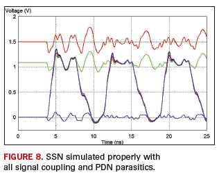
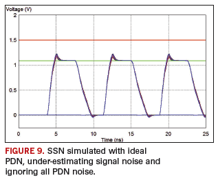
These simulations clearly demonstrate the dominant contribution of PDN effects to SSN noise. PDN noise is seen to be a significant contributor, due to both plane effects and via/trace/pad parasitics of device mounting structures. The results of Figure 9 are common to a majority of EDA signal integrity (SI) solutions because they assume an ideal PDN and do not simultaneously consider power integrity effects. Application of such SSN simulations yields an unacceptably low prediction of signal noise and completely ignores PDN noise. Coupled SI-PI simulation enables reliable prediction of signal-dependent PDN noise, which in turn can be applied to reliably predict board-level emissions under actual operating conditions – a task not practical for SI or PI simulation alone.
Conclusion
Power integrity is all about noise, with margins for both DC and AC noise contributions. In the sense that DC is just another frequency point, the vast majority of post-placement/pre-route PI simulation and measurements are performed in the frequency domain. Stackup design, VRM/component placement and current constraints for vias/planes are key issues. Pre-layout AC PI design challenges relate to crafting a low PDN impedance profile with proper placement and selection of decaps. Decap placement and selection are based on PDN resonance behaviors that are fairly easy to understand, demonstrated here or automated by EDA solutions. Post-layout verification of SI and PI are tightly coupled concerns because both are depend on signaling conditions. PDN effects play the dominant role for SSN, and reliable simulation of SSN cannot occur in their absence. pcd&f
Brad Brim has product marketing responsibility for Sigrity in the area of PCB and package simulation; This email address is being protected from spambots. You need JavaScript enabled to view it..