Process chemistry, substrate condition, mass transport and current density have a significant impact on via-filling capability.
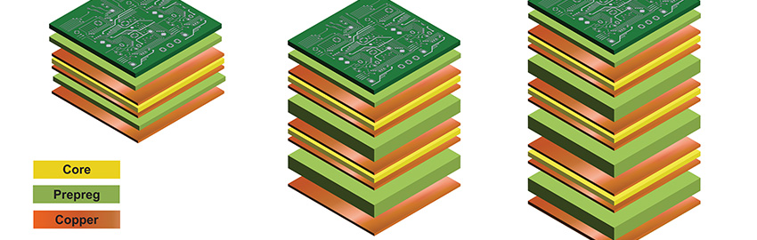
Driven by the need for increased speed, portability and wiring density, the interconnect pitch on semiconductor packages and the corresponding high-density interconnect (HDI) substrates continues to shrink. The combination of filled blind microvias and build-up technology provides a means to achieve the required wiring densities. With the rapid growth of this technology, the use of electrodeposited copper for filling blind microvias has become a widely adopted process for manufacturing HDI boards and semiconductor package substrates.
In order to produce the increasingly narrow line widths and spacing (L/S) required to route state-of-the-art packages, build-up technology is undergoing a shift from subtractive techniques toward the semi-additive process (SAP). This shift is being driven by the inherent limitations of subtractive/etch processes with regards to resolution.
Using SAP in a build-up process starts with a photoresist pattern formed after the initial electroless metallization of the dielectric material. Following electroplating and resist stripping, the use of a “differential etching” process allows for feature formation without the use of metal etch resists.
A modified SAP process, also referred to as an advanced-pattern process (APP), is often used in HDI fabrication. In this case, a laminate coated with a thin copper foil is used for the starting material, rather than a bare dielectric. Both of these processes are preferred over subtractive approaches due to their improved etch capability at feature dimensions below 40 microns.
TABLE 1 provides a technology comparison.

Electroplated Copper Via Fill
The vast majority of via fill electroplating baths are based on electrolytes consisting of copper sulfate and sulfuric acid. Combining low-cost and convenient operations, these sulfate-based systems are a well-established technology, having been used in the PCB industry for over 50 years, including 10 years in via fill applications.
A typical acid sulfate system contains copper sulfate (the primary source of cupric ions), sulfuric acid (for solution conductivity) and a chloride ion (as a co-suppressor). Of these components, copper sulfate, typically at concentrations above 200 g/L, has the most significant effect on via-filling ability.
An acid copper sulfate system, operated without additives, typically yields deposits of poor physical properties. Therefore, organic additives, typically consisting of materials described as brighteners, suppressors and levelers, are used to further refine deposit characteristics.
Suppressors, also referred to as carriers or inhibitors, are typically high molecular weight polymers that work in conjunction with small amounts of chloride to form a surface film on the plating surface, which retards the plating reaction. This limits the lifetime of individual growing grains, causing the deposit grain size to become smaller than that obtained without a carrier. Carriers are present in relatively high concentrations (≥ 500 mg/L) and show rather low sensitivity to variations in the rate of mass transferred to the surface. However, in the absence of additional additives, deposits from such formulations do not have smooth, bright surfaces.
Brighteners are typically low molecular weight sulfur-containing compounds that locally increase the plating reaction by displacing adsorbed carriers. The impact of brightener additions occurs preferentially at points of lower field density, typically in surface recesses or at the bottoms of vias or trenches. The function of the brightener is to accelerate the rate of the copper plating reaction and further refine the grain size of the deposit.
Levelers, a further class of additives, act as selective suppressors and typically operate at low concentrations (< 10 mg/L). At these low concentrations, the activity of levelers is more dependent on mass transfer then that of carriers, with the consequence that less isolated locations (such as the panel surface) are more suppressed than more isolated locations (such as the interior surfaces of vias and recesses within via hole walls).
Bottom-Up Fill Mechanism
In order for blind vias to be filled with a high quality, continuous copper deposit, the plating rate within an individual via must vary. The plating rate at the base of the via must be substantially faster than that of the remaining areas in order to avoid premature closure of the mouth of the via opening and the consequent formation of voids or seams.
Bottom-up via-filling behavior is attributed to the action of organic additives. The neutral charge suppressor rapidly forms a current-inhibiting film on the copper surface. This film has little geometric dependence due to a high suppressor solution concentration. The accelerated bottom-up fill behavior is due to a relative accumulation of brightener species at the base of the feature. As surface area in the via is reduced during deposition, the concentration of brightener species increases1, accelerating the plating rate relative to the surface. The leveler acts to suppress the plating at the corners of vias and to aid in reducing the formation of a void.
Via-filling performance may be characterized by a number of related metrics. Percent via fill (% VF) and “dimple depth” have been perhaps the most commonly used metrics used to quantify via-filling performance. The relative deposition thickness (RDT) is a more recently developed metric.
2 Defined as the ratio of the fill thickness and the copper thickness plated on the board surface, it is an improved indicator of filling performance. A conformal plating process will give an RDT value of 1, based on the definition shown in
FIGURE 1. However, even a plating formula with a filling capability of 100% may exhibit a low RDT value, perhaps as low as 2 or 3. This means that while the plating formula is able to fill the microvia in a bottom-up mode, the required surface thickness buildup of copper will be excessive. Higher surface thicknesses of copper detract from the ability to subsequently etch fine circuit traces.

In addition, for pattern plate processes, individual pad and trace features will not be perfectly flat. Trace profile is used as the general term to describe such deviations from planarity, and depending on the chemistry and process conditions, either convex or concave profiles may be formed. Customer specifications for trace profiles are typically expressed as the maximum difference in height between the edge and the center of a feature.
Customers are demanding continuously improved surface planarity, whether expressed as reduced dimple depth, improved trace profile or better surface distribution.
Poor planarity can potentially impact reliability in a number of ways. Dimpling can increase the effective aspect ratio of the next via formed within a stack, may lead to interfacial voiding during subsequent application of build-up dielectric and increase risk of solder joint voiding on via-in-pad structures. Poor feature profile or surface distribution may lead to unacceptable variability in trace impedance, adversely affect solder mask application and may also affect wire bond consistency.
Copper Via Fill Development
The product development objectives focus on maximizing via fill and through-hole throwing power, while minimizing thickness variation across the substrate surface. Commercially desirable via-filling processes will, therefore, demonstrate a combination of high-filling performance, low dimple and low feature profile, with uniform surface distribution and high through-hole throwing power. The exact target values for these metrics will depend upon specific application and end-user requirements. However, for purposes of benchmarking development progress, the following performance targets should be used.
- HDI: 75 μm to 125 μm dia x 50 μm to 100 μm deep, target <10 μm dimple @ 20 μm surface Cu.
- Package Substrate: 50 μm to 75 μm dia x 30 μm to 40 μm deep, target < 5.0 μm dimple @ 15.0 μm surface Cu.
- Operating current density: 10 ASF to 20 ASF for panel and pattern plate, compatible with insoluble anodes.
- Through hole: 0.15 mm to 0.3 mm dia x 0.8 mm to 1.0 mm, target ≥ 80% throwing power.
- High knee thickness.
- Trace and pad profile exhibit a convex track of less than 5 μm.
- Panel surface distribution Coefficient of Variance (CV x 100%) ≤ 10%.
- Cyclic Voltammetric Stripping (CVS) analysis for all components.
Next-generation HDI via-filling systems should be capable of plating a wide range of products with a single process chemistry, irrespective of microvia dimension or aspect ratio. By using specific recipes of current density and/or solution flow, the performance for different classes of product can be optimized.
During the development program, extensive screening was conducted on various classes and combinations of additives, carriers and levelers for via filling, trace profile and through-hole throwing power performance. Candidate materials were further optimized with inorganic chemistry component concentration. Test vehicles included panel and patterned substrates featuring CO
2 and UV laser-ablated blind microvias ranging from 75 μm to 150 μm in diameter and mechanically drilled through holes ranging from 0.15 mm to 0.30 mm in diameter, in 60-μm- and 100-μm-thick panels.
PCD&FREFERENCES1. T.P. Moffat, J.E. Bonevich, W.H. Huber, A. Stanishevsky, D.R. Kelly, G.R. Stafford, D. Jossel, “Superconformal Electrodeposition of Copper in 500 – 90nm Features,” J. Electrochem. Soc., Vol 147, 4524 (2000).
2. W.P. Dow, M.Y. Yen, M.J. Lefebvre, “Studies of Microvia Filling Mechanism and A Novel Cu Plating Formula,” IMPACT 2007.
Leon Barstad is an engineer A;
This email address is being protected from spambots. You need JavaScript enabled to view it.,
Luis Gomez is a senior scientist;
This email address is being protected from spambots. You need JavaScript enabled to view it.,
Elie Najjar is a senior engineer;
This email address is being protected from spambots. You need JavaScript enabled to view it. and
Mark Lefebvre is research manager;
This email address is being protected from spambots. You need JavaScript enabled to view it.. They are all with Dow Electronic Materials, The Dow Chemical Company.
Ed. Note. Part 2 of "Electroplating for HDI and Packaging Substrates" will continue in the September issue.