-
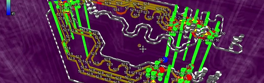
Material Selection for High-Speed PCBs
Consider return loss and insertion loss – but don’t stop there. READ MORE...
-
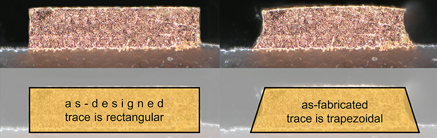
Characterizing Etchback and Dielectric Loss Tangent
Fabrication-aware simulations to aid PCB design success. READ MORE...
-
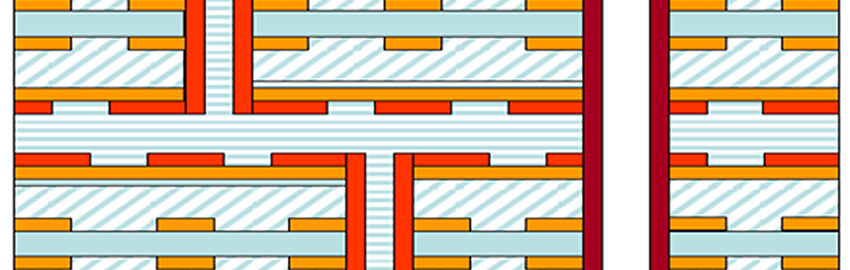
Sequential Lamination in PCB Manufacturing
Manufacturing high-layer count boards. READ MORE...
-
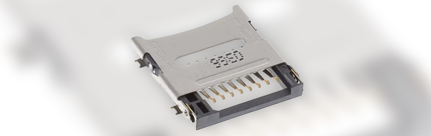
Implementing Flash Memory in PCB Design
Routing flash has EMI implications. READ MORE...
Homepage Slideshow
Material Selection for High-Speed PCBs
Consider return loss and insertion loss – but don’t stop there.
Characterizing Etchback and Dielectric Loss Tangent
Fabrication-aware simulations to aid PCB design success.
Sequential Lamination in PCB Manufacturing
Manufacturing high-layer count boards.
Implementing Flash Memory in PCB Design
Routing flash has EMI implications.


