-
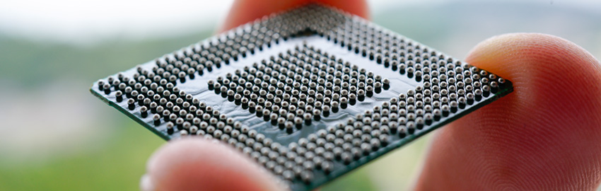
What is Ultra HDI?
With Ultra HDI, small features come with big decisions. READ MORE...
-

The Critical Nature of PCB Stackup
The stackup supports every layer above it. READ MORE...
-
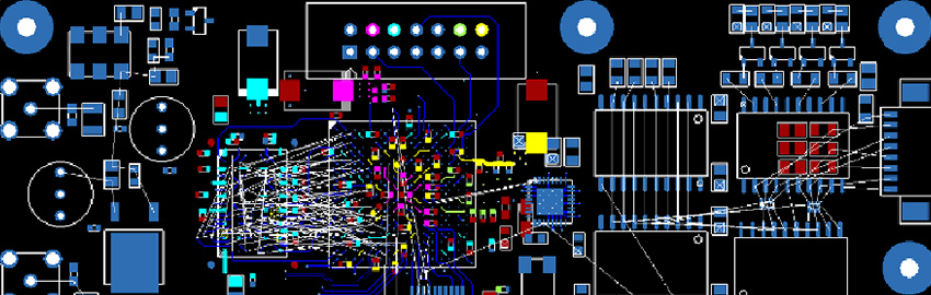
The PCB Design Review Process
A structured design review process ensures alignment. READ MORE...
-
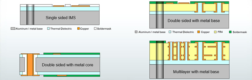
Metal-Core PCBs and Thermal Management
Catch heat at the board. READ MORE...
Homepage Slideshow
What is Ultra HDI?
With Ultra HDI, small features come with big decisions.
The Critical Nature of PCB Stackup
The stackup supports every layer above it.
The PCB Design Review Process
A structured design review process ensures alignment.
Metal-Core PCBs and Thermal Management
Catch heat at the board.


