Don’t ignore the stackup.
The majority of PCB articles concern standard boards, often stuffed full of complex components, and the latest high-speed circuitry and the problems that brings to the table. Flexible PCBs are not talked about much in day-to-day literature, but the truth is without them most of the devices we have come to depend on would not exist – at least not in the tiny package we know and love.
From smartphones and tablets to household appliances to automobiles, flexible PCBs connect rigid boards in ways to make the final package smaller, lighter, more reliable, and more cost-effective. Do flexible PCBs have special design concerns that rigid boards do not? Absolutely! So, let’s take a look at some of the
benefits and challenges of flexible PCBs … or just “flex.”
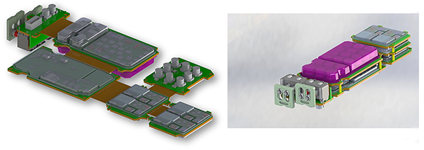
Most commonly, flex is used as an interconnect between two or more rigid PCBs. The most common reason to employ flex is to permit those rigid PCBs to be stacked or otherwise configured in three dimensions (FIGURE 1).

Figure 1. Flex permits flat, rigid PCBs to be connected together in an efficient, cost-effective 3D shape.
With accurate design and automated production, flex circuits can also eliminate human errors from hand-built wire harnesses that show up in assembly. Flex systems also require less manual labor during assembly and can reduce production errors, therefore decreasing assembly time and costs. Durability is greater than wire harnesses as well; a flexible circuit can move and flex up to 500 million times without failure in designs that have moving parts. Plus, the exceptional thermal stability of polyimide also permits circuits to withstand applications with extreme heat.
Figure 1 shows one of the common flex designs: a flex cable. A flex cable is a miniaturized form of a ribbon cable that is flat and flexible. The cable consists of a flat and plastic film base, with multiple metallic conductors bound to one surface. Often each end of the cable is reinforced with a stiffener for insertion of components and to provide stress relief.
Another common form is rigid-flex. A rigid-flex design consists of multiple innerlayers of flexible circuits and rigid regions typical to everyday PCBs. These are often found in cellphones, LCD TVs, antennas, laptops, and more.
Advanced flex is a single PCB design that incorporates multiple stackup changes, as well as components placed on the flexible substrate. A flex system is a combination of multiple flex types.
Flex Design Challenges
Quite a few challenges are specific to flex circuits. The most important ones are briefly discussed below.
Stackup. Defining the flexible and rigid regions correctly within the stackup is absolutely essential. Three popular stackup configurations with flex design include:
- Embedded coverlay, where the cover layer is laminated to the rigid section.
- Bikini cover layer where the cover layer is applied only to the flexible regions and is defined only a small amount into the region to anchor the material.
- Book binder flex, which needs the user to specify an additional length to be added to the bending radius.
Bend area. Defining a bend area is critical in a flex design. A bend area drives all functions related to the bend from the radius, angle and design rule checks. The bend area drives the 3D visualization and DRC. For example, design rules can detect vias placed in bend areas or traces that are not perpendicular to the bend area, both of which can cause reliability issues.
Circuitry placement. Circuitry layout makes or breaks a PCB. Curved traces cause lower stress than angled ones. Traces should also be kept perpendicular to the overall bend and, if placed on a flex PCB with two or more layers, staggered on the top and bottom. To prevent potential tearing of the flexible board, use drill holes to terminate.
Complex 3D shapes. A challenge in routing flexible board sections lies in what often are very complex shapes that restrict routing channels and require routing busses on flex cables such that they follow the shape of
the package.
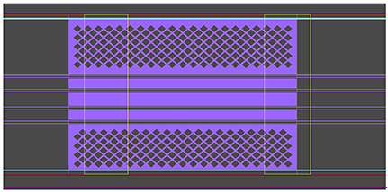
Fill planes. Not only must routing quality be taken into account, but the correct plane fill can seriously affect circuit reliability. A solid plane fill can add additional metal strain, potentially causing issues. Cross-hatched patterns provide reliable connectivity without increased weight and strain. Cross hatches should be exactly 45˚ to the bend line (FIGURE 2).

Figure 2. Cross hatches should be applied at 45 degrees to the bend line of the flex.
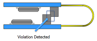
Handoff to the manufacturer. Before data are sent to fabrication, use DRCs to identify critical issues within the design (FIGURE 3). Updated design rule checks identify potential reliability and design issues within the flexible region. Checking fabrication rules can eliminate potential problems before the flex gets to the manufacturer.

Figure 3. Design rule checks and 3D visualization can detect problems before any hardware is built, potentially saving a great deal of cost and time.
Flex circuitry is not overly difficult to design, but does have its set of challenges. Correctly addressing those challenges will result in a flex that is reliable and cost-efficient.
Alex Grange is technical marketing engineer at Mentor Graphics (mentor.com); This email address is being protected from spambots. You need JavaScript enabled to view it..


