
Reusing MCAD data eliminates duplicate work and errors.
When we envision a completed PCB, we almost always think of a nice rectangle. While most designs are indeed rectangular, many designs require boards of unusual shapes that are a bit more difficult to work with. This column describes how to deal with unusual shape requirements for PCBs.
Trends continue with ever-shrinking PCB sizes containing ever-increasing functionality – all while designs have become more complex with increasing clock speeds. So let’s examine how to handle boards that are no longer simple shapes.
FIGURE 1 shows the outline of a simple PCI board. PCI board shapes are generally fairly easy to create in most EDA layout tools, as shown with the example.
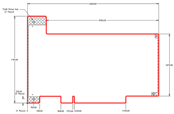
Figure 1. Outline of a common PCI board.
When a board outline needs to fit into a complex enclosure with height restrictions, however, life is not so easy for PCB designers because the tools are not designed to function in the way mechanical CAD systems function. FIGURE 2 shows a complex board for use in an explosion-proof housing with many mechanical restrictions. Trying to recreate this information in your EDA tool may take a long time and is not productive. More likely, a mechanical engineer has already created the housing, board outline, mounting hole locations and height restrictions that the PCB designer needs. Even seemingly not-too-complex board outlines such as the one in FIGURE 3 may take longer than anticipated to recreate due to the arcs and radii incorporated into the board.
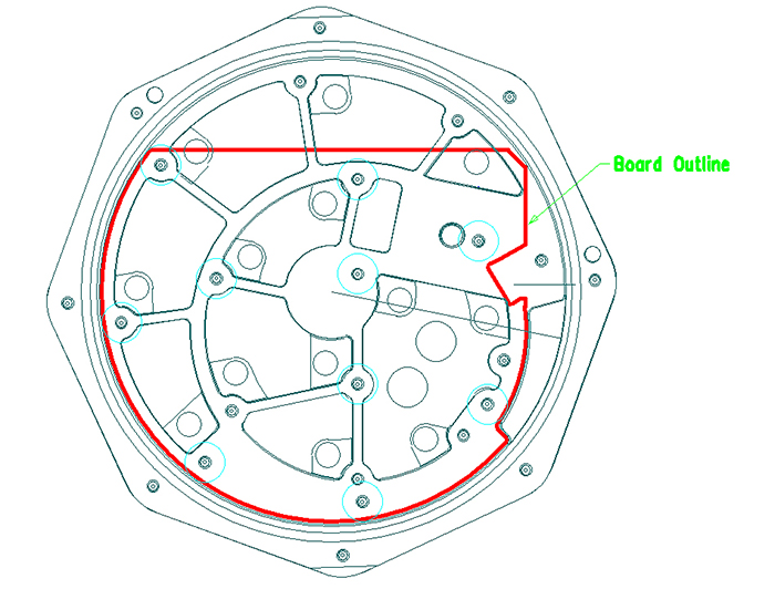
Figure 2. In this example, a PCB must be designed to specific mechanical specifications so that it can fit inside an explosion-proof container.
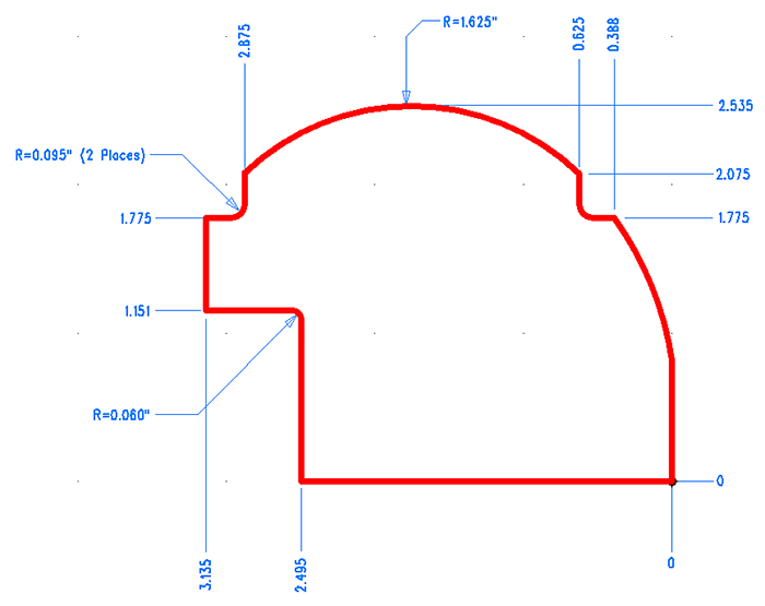
Figure 3. Multiple arcs and different radius curves can take a long time to design.
These are just a few examples of complex board shapes. However, if you look at any of today’s consumer electronics, you will be surprised how much engineering goes into stuffing all the capabilities into a small package, which isn’t always rectangular. Smartphones and tablets are applications that quickly come to mind, but there are many examples.
If you have returned a rental car, you probably have seen attendants use handheld scanners to read vehicle information and wirelessly communicate with the office. The device also incorporates a thermal printer for instant receipt printing. Virtually all of these devices employ rigid/flex boards (FIGURE 4) where traditional PCB boards are interconnected with a flexible printed circuit that can be folded into small spaces or traversed through tight openings.
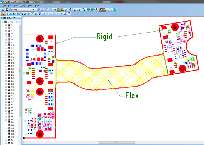
Figure 4. Rigid/flex boards allow the maximum use of available space.
Avoid recreating existing data. So the question is, How can the mechanical engineering specifications that have already been defined be imported into the PCB design tool? Reusing this data from mechanical drawings eliminates duplicate work and more importantly eliminates an opportunity to introduce human errors. That problem is solved in the form of DXF, IDF or ProSTEP formats that can import all of the information into PCB layout software that will save a great deal of time and eliminate possible human-introduced errors. Let’s examine these formats one by one.
Drawing Exchange Format (DXF). The DXF format is the oldest and most widely used format to exchange data between mechanical and PCB design domains in electronic format. It was started by AutoCAD in the early 1980s. This format has predominantly been used for two-dimensional data exchange. The vast majority of PCB tool vendors support this format, and it does simplify data exchange. DXF import/export needs additional capability to control layers, different entities, and units that will be used during the exchange. FIGURE 5 is an example of importing a very complex board outline in the DXF format.
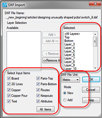
Figure 5. PCB design tools, such as PADS illustrated here, need to be able to control the various parameters required with the DXF format.
Intermediate Data Format (IDF). A few years ago, three-dimensional capabilities began to appear in PCB tools, and there was a need for a format to communicate 3D data between mechanical and PCB tools. Mentor Graphics created the IDF format, and it was widely accepted to transfer board and component information between PCB and mechanical tools.
While DXF contains board size and thickness, IDF uses X and Y location of parts, their reference designators, and the part’s Z axis for height. This format greatly improved the ability to visualize PCBs in three dimensions. Additional information for keepouts with height restrictions for both the top and bottom of the board were also possible to include into IDF files.
In a similar way to the DXF parameter settings, design tools need an ability to control what will be included in the IDF files (FIGURE 6). If some components did not have height information, IDF export has an ability to add missing information during its creation.
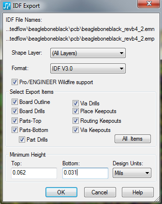
Figure 6. Parameters can be set in the PCB design tool.
Another advantage of IDF is that either party can move components to a new location or change the board outline and create a different IDF file. The disadvantage of this approach is that the entire file representing board and component changes needs to be re-imported, and in some cases it may take a long time due to the file sizes. Also, it’s difficult to determine from the new IDF files what changes have been made, especially on bigger boards. Users of IDF eventually created custom scripts to identify the changes.
STEP and ProSTEP. Seeking an improved way to communicate 3D data, the STEP format was born. The STEP format can communicate board size and component placement, but more important, the components are no longer simplistic shapes with one height. STEP component models are a detailed, complex representation of a part in 3D. Both board and component information can be passed between PCB and mechanical designers. Yet, there was still no mechanism to track changes.
To improve on the STEP file exchange, the ProSTEP format was introduced. This format can move the same data as IDF and STEP, with a great improvement: It can track changes and provide the ability for either discipline to work in their native system and review any change after establishing a baseline. In addition to seeing
just the changes, both PCB and mechanical engineers can approve all or individual component change in placement, board outline modifications. They can also counter propose different board sizes or component locations. This improved communication established an engineering change order (ECO) ability between ECAD and mechanical groups that had not existed (FIGURE 7).
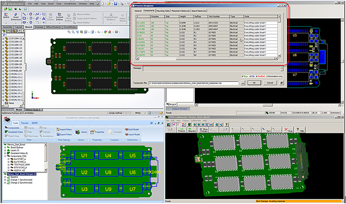
Figure 7. Changes are proposed, viewed on native tools, and approved or counter solutions proposed.
The majority of ECAD and mechanical CAD systems now support ProSTEP. More important, an engineer can create a complex board outline with additional restrictions once and pass this information electronically, thus realizing time savings with no possibility of someone reinterpreting the board size incorrectly.
If you have not used these data formats to exchange information via DXF, IDF, STEP, or ProSTEP, you should examine their usage. Look into using this electronic data exchange and stop wasting time recreating complex board outlines.
Yan Killy is technical marketing manager, PADS products at Mentor Graphics (mentor.com); This email address is being protected from spambots. You need JavaScript enabled to view it..


