The eye can be improved through additional caps or staggering signal toggle.
Digital designers are used to noise affecting designs from all different kinds of sources. With fast data rates running on parallel busses, designers now need to be concerned about the noise coming out of the chip itself. One such kind of noise, simultaneous switching noise (SSN), occurs due to the simultaneous switching output (SSO) of buffers on a driving chip.
When a driven signal inside the chip transitions states, it consumes power from the rail. If a sufficient number of signals switch simultaneously, the rail voltage can droop due to the inability to supply adequate current for all the switching outputs. This could happen because the capacitors on the power distribution network (PDN) that are providing the current are too far away, or because those capacitors have been laid out in a way which causes them to have a high series inductance.

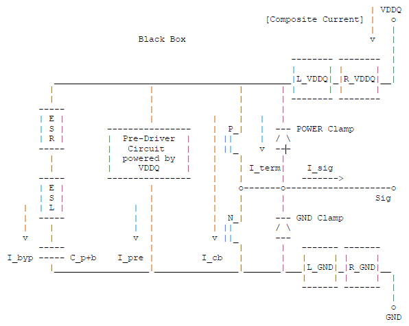
Figure 1. IBIS 5.0’s Power-Aware features.
This droop in rail voltage results in the buffer driver’s output signals being distorted. This is similar to crosstalk-induced noise in that the switching of one signal can also cause variations in the output of another signal.
Accurately simulating the current draw of one driven signal on the voltage rail and the subsequent effect on other drivers requires information regarding the buffer’s behavior. One option would be Spice models. Alternatively, IBIS permits simulations that are much faster than Spice at a comparable level of accuracy, and are therefore a popular standard for simulation. IBIS 5.0 supports the data structures needed to simulate this “power-aware” topology.
SSN is particularly relevant for high-speed parallel busses such as DDR4. With parallel busses, each bit can act independently of the others. This can cause large loads on the power rails when the signals all switch in unison.
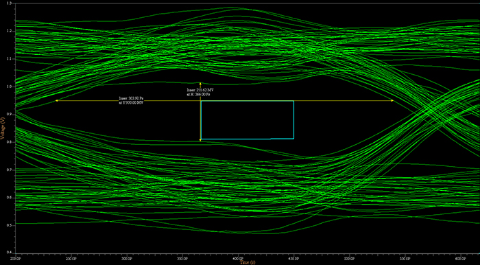
To illustrate the effects that a PDN can have on signals, consider a setup of a single DDR4 byte lane running at 2400 Mt/s, with each signal running a unique random sequence. In this simulation setup, the package capacitor is not loaded. This removal of a major source of power for the higher frequency transitions (artificially) exacerbates the SSN effect. In FIGURE 2, the eye for DQ0 does not have a lot of margin around the eye mask. This is not a very good situation.

Figure 2. Poorly designed PDN.
If, instead of a random sequence, we switch the entire byte land with the same sequence, the situation gets even worse. Using this technique we can see the worst case effects of SSN, that is, when all the signals are toggling in unison and placing a significant load on the voltage rail. As seen in FIGURE 3, the eye for DQ0 gets much worse if all the bits are toggling with the same data pattern. In this case the eye closes almost completely.

Figure 3. Worst case bit pattern with a poorly designed PDN.
Improving the PDN. Next, let’s insert the 4.7uF package capacitance that was removed to begin with. This should be a low-ESR capacitor and should be placed so that the inductance-causing loop area is minimized.
In this setup, all the signals continue to toggle with the same bit pattern. So, this is the worst case situation with the package capacitor inserted. This DQ0 waveform in FIGURE 4, while better than that generated without the package capacitor in Figure 3, is only barely passing the eye mask.

Figure 4. Worst case bit pattern with improved PDN.
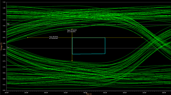
In a more realistic situation, the signals would indeed be independent of each other. Using unique random bit stream for each signal, we get the DQ0 eye shown in FIGURE 5. The DQ0 eye improves dramatically. The smallest eye height in the mask region is now 275.5mV, better than the 211mV eye-height in the setup with the package capacitor where all the signals switch identically (Figure 4), and better than the 237mV eye-height with the setup where the package capacitors have been removed, but the signals toggle independent of each other (Figure 2).

Figure 5. Unique, random bit patterns for all signals with improved PDN.
Data bus inversion. Another way to improve the eye, as we’ve seen, is to ensure all the bits don’t toggle at the same time. In a DDR4 design, the Data Bus Inversion (DBI) optional feature can do just that. If DBI is enabled, the driver (the controller during a write or DRAM during a read) counts the number of 0s (logic low) bits. If the number of bits driving 0 in the lane is five or more, then the entire byte is inverted, and a ninth bit indicating DBI is asserted low. This ensures that out of the 8 DQ bits and the ninth DBI bit, at least five bits are 1 during any given transaction. This also ensures that out of the entire data lane, the maximum total number of signals transitioning is either five 1s to nine 1s or vice versa. There can never be a situation where all bits go from 0 to 1 or from 1 to 0.
So, if we run the same data bus with data patterns which would be the output of the DBI logic, we get the waveform for DQ0 in FIGURE 6. The eye-height for DQ0 in this case is over 315mV, which surpasses all the other conditions. Now, since DBI is data-dependent, the benefits of DBI may vary and need to be analyzed before implementation.

Figure 6. DBI processed bit patterns, with improved PDN.
What we can gather from the above data is that the eye can be improved by adding appropriate package capacitors, or by ensuring that signals don’t all toggle identically. Ensuring all the signals don’t toggle identically is one of the benefits of enabling the DBI option in DDR4.
With a good design of the PDN, and possibly selecting the DBI feature in DDR4, SSN shouldn’t be a concern in the design.
Nitin Bhagwath is high speed product manager at Mentor Graphics (mentor.com); This email address is being protected from spambots. You need JavaScript enabled to view it..


