ECTC showed fan-out wafer level packaging has many fans.
Orlando in May hosted the 64rd Electronics Components and Technology Conference (ECTC), where more than 1,000 attendees from 33 countries gathered to discuss recent developments in semiconductor packaging, assembly, materials and manufacturing.
While many presentations reported progress along the road to 3D IC manufacturing with through silicon vias (TSVs), the holy grail of stacking dies with different functions remained as elusive as Piglet – a shy creature who rarely makes an appearance in Disney’s Magic Kingdom theme park. The need for 3D ICs remains constant, as companies ponder the cost of lithography at silicon technology nodes of 10nm and below.
Many research institutes such as Fraunhofer, IMEC, ITRI, NCAP, and others provided insight into process improvements that have taken place in the last year. Continued improvements in copper via reveal were reported, along with new materials, and equipment for wafer thinning, focusing on the debond step. Applied Materials announced its Ventura oxide and barrier coverage PVD system designed specifically for TSVs, providing better barrier and seed coverage on the walls, bottom and corners of copper vias, with improved speeds as a result of thinner films. Sachem and Solid State Equipment (SSEC) announced the release of Reveal Etch, a novel wet chemistry designed to enable a single-step silicon etch/TSV reveal process. SSEC worked with Sachem to develop this proprietary aqueous chemistry, which is residue-free and does not contain potassium. After years of dedicated R&D for this 2.5D/3D application, SSEC has integrated all the key components in a single tool – silicon thickness metrology for accurate endpointing determination, wet etch with a spin-etch chemistry to avoid using separate CMP equipment, a final etch with the chemistry to uniformly expose the TSVs, and wet cleaning. IBM provided information on use of a laser debond process in wafer thinning. IBM, Disco and Lasertec presented a TSV revealed process based on a metrology tool that uses IR reflectance to measure the silicon thickness remaining at the bottom of the TSV and backside surface of the wafer, coupled with a mechanical grinding and chemical mechanical polishing to expose the vias. Dow Electronic Materials discussed Pb-free solder plating developments for micro bumps.
A number of presentations focused on the potential for glass interposers, but whether the “glass” is half-full or half-empty was not clearly answered. Researchers from Korea Electronics Technology Institute, Georgia Institute of Technology, ITRI, RTI, NTK, Unimicron and other organizations clearly demonstrated that much progress has been made in the last year in via fabrication and other process areas. Material developments enabling fine features on large areas have been introduced. For example, Atotech and Georgia Tech demonstrated fine feature (3 to 5µm RDL) for panel-based interposers. While there are indicators that the equipment infrastructure is developing with new lithography developments from Ultratech and a foray into the space by Rudolph, a mature supplier base is still several years away. Corning provided multiple presentations in a theater setting, exploring potential applications for glass extending beyond just interposers, and Triton Microelectronics continued to discuss glass as more than just a replacement for silicon interposers.
Organic interposers continue to gain momentum as an interposer option. Presentations from Amkor, GlobalFoundries, Kyocera, NTK, Shinko Electric and Unimicron highlighted the latest developments, while companies provided insight into their activities in the Technology Corner exhibits. Despite all these new developments in alternatives, there were still plenty of discussions on silicon from GlobalFoundries, SPIL and UMC, to name a few.
FO-WLP a hot topic. The session that covered fan-out wafer level packaging (FO-WLP) proved to be the “hot topic,” with more than one-fifth of the attendees crowding into an afternoon session to hear the latest developments. Qualcomm described the limits of moving to finer-pitch balls on WLPs, leading the way for a discussion about the advantages of edge protection in Stats ChipPAC’s encapsulated eWLCSP FO-WLP version. Nanium explained how a new dielectric material has enhanced reliability of its FO-WLP. Panel production, also a form of embedded die, was introduced with Fraunhofer IZM and the Technical University of Berlin’s development of a 24" x 18" panel production line. SPIL also echoed the shift to panels by describing its panel FO-WLP research. A presentation on packaging large die in an FO-WLP (10 x 10 and up to 13 x 13mm) provided promise for the expansion of FO-WLP past its traditional 5 x 5mm die size. The session concluded with a discussion of a new application demonstrating a 3D rectangular waveguide integrated into Infineon’s eWLB version of the FO-WLP.
Substrate warpage as an assembly issue for flip chip on organic interposers and silicon interposers was an important topic discussed across many sessions as an assembly issue for flip chip on organic interposers and silicon interposers. Solutions such as new materials and flip chip assembly processes were described. A number of presentations highlighted progress in glass interposers, including improvements in via fabrication. New bump fabrication methods, materials and metallurgies included developments for traditional flip-chip CSP and BGAs, as well as micro bumps for 2.5D and 3D IC applications. Nanoparticles are appearing in everything from bump metallurgies to underfill and thermal interface materials. Carbon nanofibers are appearing in a variety of material formulations. Developments in anisotropic conductive films and pastes, including formulations for chip-on-glass (CoG), were discussed.
Special session discussions. The Flexible Electronics: Packaging Technology and Application Trends organized by the Fraunhofer EMFT and University of Berlin included a lively discussion on technology trends, setting the stage for a number of conference papers on wearable and stretchable electronics in products ranging from skin-mounted electronics to new manufacturing methods with conductive inks and nanoparticles. The Wireless Power Transfer Systems session included discussions on energy harvesting to enable improved battery life. A session on Silicon Photonics provided insight into the possible applications. The session on Packaging Influence on System Integration and Performance included topics such as a system-level design approach and future requirements. Based on the panel discussion and many conference papers, die partitioning resulting in the creation of a multichip module is likely to reemerge as the solution to many system needs. Future package designs are likely to include a system-in-package (SiP) choice. The final night session discussed the latest advances in organic interposers, including insight into Kyocera and Shinko Electric’s paths to less than 5µm line width and spaces in organic substrates. Potential users such as IBM and Xilinx provided insight into the possible roadmaps for organic substrate technology.
Developments in LED packaging and assembly, including introduction of materials such as die attach and improved thermal designs, were discussed. Wafer-level packaging methods for LEDs were also described.


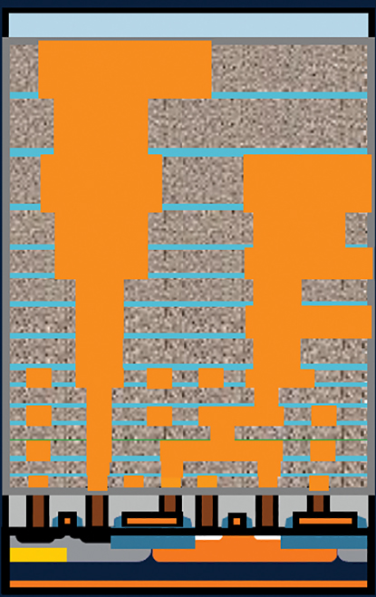
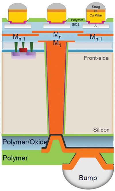
Figure 1. TSV structures are 1000 times deeper than copper vias.
E. Jan Vardaman is president of TechSearch International (techsearchinc.com); This email address is being protected from spambots. You need JavaScript enabled to view it.. Her column appears bimonthly.


