Designs with analog, digital and RF features challenge the PCB designer to reduce noise, improve EMI performance and lower distortion.
The layout of an efficient mixed-signal design can be both time consuming and challenging. However, diligently working on this type of layout can result in a system with less crosstalk, more noise immunity and better EMI performance. The PCB industry continues gearing toward higher speeds, miniaturized components and denser circuits, and consequently, the coexistence of digital and analog technologies in close proximity has become unavoidable. Add to this an element of RF circuitry, and the designer’s job has just become a bit more difficult.
Digital and analog circuits are similar in the fact that they both rely on voltage variations to transmit information, but the difference lies between voltage amplitude levels and noise immunity. Digital circuits operate on distinct voltage levels, and a digital driver is designed to create a voltage level higher than that required by the receiver. As long as this threshold voltage is achieved, the digital circuit is functional. Hence, these circuits are less susceptible to noise and distortion. Digital circuits are also noisier than their analog counterparts.
On the other hand, analog signals convey information in the form and the shape required by the receiver. Any amount of difference in this information can make the device function improperly. Analog signals usually have low amplitudes, as well as a high signal-to-noise ratio (SNR) that is more difficult to achieve.
RF signals are similar to analog circuits with respect to signal propagation. However, these signals operate at specific frequencies that usually depend on odd-shaped circuits etched on the PCB. These circuits are the least resistant to outside noise, so it is important to isolate them from digital circuits for proper operation.
The layout of a mixed-signal PCB poses many challenges to the OEM design engineer and the PCB designer. It is incumbent on both parties to keep in close coordination throughout the project because the more information that can be provided to the PCB designer, the better. It’s also in the best interest of the PCB designer to be aware of and educated on the different types of circuitry that will be present on the board layout. In other words, he or she should be able to identify the digital, analog and RF circuitry before the start of the layout.
Component Placement
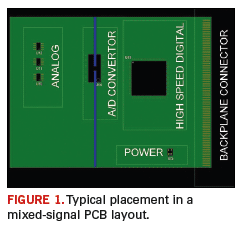
Component placement is the most critical aspect in any mixed-signal design, and its effects will trickle down to all the steps following it. If ample time and thought are given at this stage, it will make life easier for the PCB designer. Prior to the start of the layout, the PCB should be divided into the subsections shown in Figure 1.

High-speed digital circuits will have fast switching times and should be placed closer to the connectors and away from any analog circuitry because low-level analog signals are most sensitive to the switching noise of digital circuits. Generally, lower speed digital circuits will include devices that interface between digital and analog circuits, including A/D convertors, DACs and MCUs. These circuits are placed between high-speed digital circuitry and analog circuitry.
Analog circuits are most susceptible to EMI and crosstalk, therefore, as a group, their components should be placed close to each other in order to avoid long signal routes. Placing analog circuits away from digital circuits will also minimize the noise being injected from the digital returns through the ground planes. Noisy circuits include power supply, relays and high-current switches. Generally, these circuits should be placed as a block, separate from all other subsystems.
Grounding Scheme
Suffice it to say that grounding is the heart of a mixed-signal layout. It can mean the difference between a product that meets all requirements and one that is subpar. The ground plane not only provides a return path to all the signals, whether they are digital or analog, but it also is a reference voltage to all the subcircuits in a PCB system. A poor ground layout will create problems such as reflections, crosstalk, EMI issues and distortion, but the best and simplest technique to avoid such problems is to provide a continuous ground plane to all digital and analog circuits. This will not only provide a low inductance return path to all the signals, but will also reduce ground bounce.
Secondly, the analog and digital ground planes should be partitioned from each other, providing little chance of interference between the returns of the two subsystems. This may be crucial for very dense mixed-signal layouts where the digital and analog circuits are placed in close proximity due to space constraints. These two separate ground planes are connected at one point, typically below the device that interfaces the two systems, for example A/D. Grounds from the noisy power supply section should also be separated through ferrite beads to filter the high frequency switching noise.
Power Supply Decoupling
A decoupling system provides a low impedance power system on the board, as well as meeting every device’s switching needs. This is true for both digital and analog circuits. All devices, whether digital or analog, have special decoupling requirements. If the rise time is short, a significant voltage drop can result across the inductance path between the power supply and devices. Moreover, if a high pin count BGA is used, there can be a substantial amount of transient current that flows through this path causing a wide range of problems– from slowing down the propagation time to false triggering.
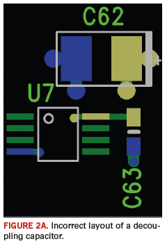
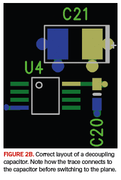
Decoupling capacitors are placed between the device and the stray inductance that can contribute to ground bounce. Usually, larger ones are used for a bulk charge and, smaller ones for a faster response that provides the switching requirements. That is why the smaller caps are placed closest to the power pin of any device. Power and ground planes can also be used to provide the small, but very fast, planar capacitance.
Here, the small distance between the adjacent power and ground plane provides the capacitance. Figure 2A shows an incorrect layout of a decoupling capacitor, while Figure 2B shows a correct layout. Note that placing a via at the opposite side of the capacitor and closer to the device pin kills the real reason behind using the decoupling capacitor in the first place.


The power supply area should also have sufficient copper to avoid any inductance build up. A generous use of ground vias in this area helps in localizing the switching noise of the regulator, and it also has heat-sinking applications.
Routing
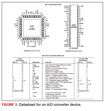
Once the placement of the different subsections is finalized and a good grounding and power supply decoupling is achieved, routing is the final step of the signal layout. Laying out signal traces at the digital/analog junction is most critical. It is incumbent on the PCB layout designer to study the datasheet of an A/D converter device in order to isolate digital and analog signals, as shown in Figure 3.

Digital traces should not run parallel with the analog traces in order to avoid any inductive crosstalk, and if these traces are routed in adjacent layers, the PCB designer should make sure that they run perpendicular to each other while passing. This will keep the capacitive crosstalk between the two to a minimum.
Another important step is to route digital and analog signals over their respective planes. These signals must never cross plane boundaries, otherwise they will inject noise into the unrelated plane, thereby defeating the purpose of the split in the first place. It is also critical that all sensitive signals are shielded from the rest of the circuitry by running fat ground traces on either side of these signals. Stitching these guard traces by vias at regular intervals will ensure that all stray currents are in sink to the ground away from the sensitive signals.
Conclusion
As the electronics industry moves towards more compact products and the domains meet, mixed-signal layout will only become more complicated. Miniaturized products will mean compact layouts. A well-designed, mixed-signal PCB can be time consuming and challenging, but it is an investment that cannot be overlooked. The above layout strategies have been presented as rules of thumb to achieve an end product with reduced noise, better EMI performance and less distortion. Every product is different, and depending on the mix of the different technologies, layout strategies may differ from one product to the next. PCD&F
Syed W. Ali is a certified interconnect designer and layout engineer at Nexlogic Technologies Inc. He can be reached at This email address is being protected from spambots. You need JavaScript enabled to view it..


