-
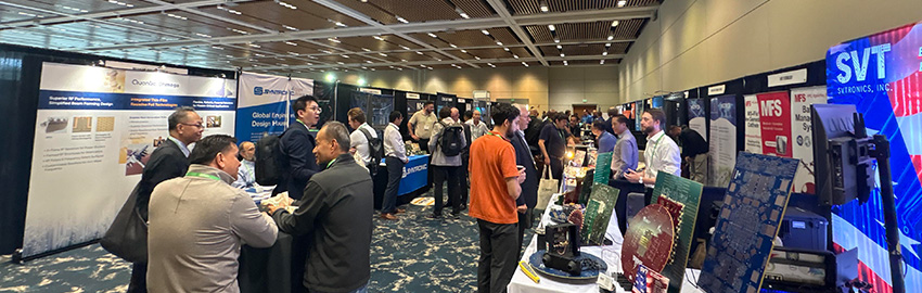
The Trade Show Connection
Finding community amid chaos. READ MORE...
-

Understanding ANOVA
Analyzing process data for accurate, defensible decisions. READ MORE...
-
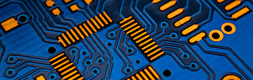
High Yield Design Practices
Building with manufacturing limits in mind. READ MORE...
-
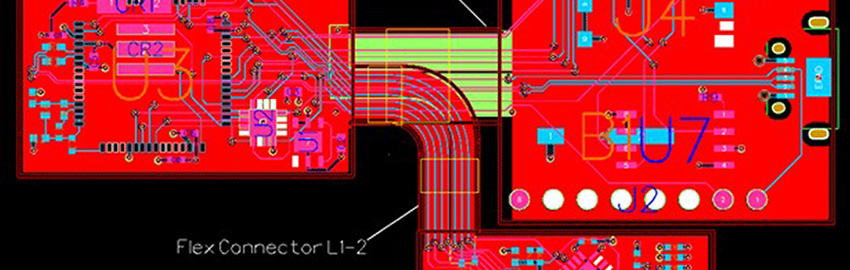
Rigid-Flex Design
Rigid-flex technology is redefining electronics design. READ MORE...
-
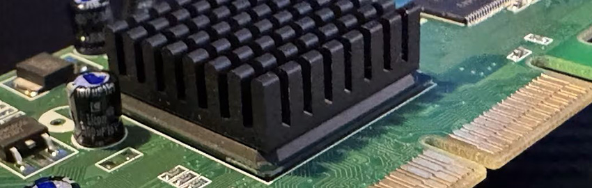
PCB Thermal Challenges
When passive heat management isn’t enough. READ MORE...
-
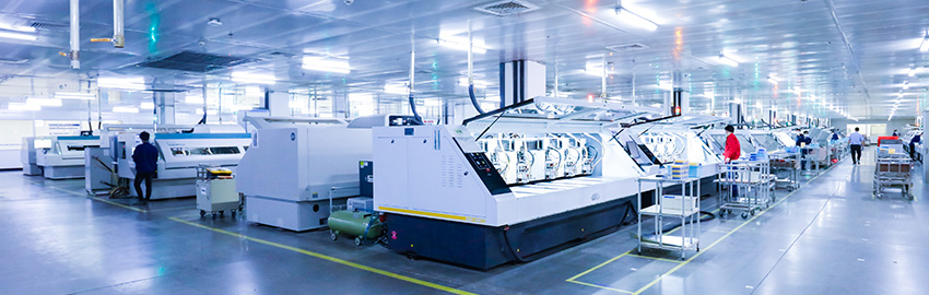
NTI-100: The World’s Top PCB Fabricators
The changing map of PCB production. READ MORE...
Homepage Slideshow
The Trade Show Connection
Finding community amid chaos.
Understanding ANOVA
Analyzing process data for accurate, defensible decisions.
High Yield Design Practices
Building with manufacturing limits in mind.
Rigid-Flex Design
Rigid-flex technology is redefining electronics design.
PCB Thermal Challenges
When passive heat management isn’t enough.
https://pcdandf.com/pcdesign/index.php/current-issue/241-designer-s-notebook
NTI-100: The World’s Top PCB Fabricators
The changing map of PCB production.


