Automation ensures new configurations are communicated and the design is synchronized.
Today’s PCB designs span a wide gamut. Designs may be as simple as a small PCB in a garage door opener or kitchen appliance, or as complex as dozens or hundreds of interconnected boards in a blade server, or it may be both small and complex, such as a smartphone. Those designs at the complex end of the spectrum push a number of design envelopes. Size is miniaturized to the extent that signal integrity and thermal management become issues. Speed is maximized to the point that tools once reserved solely for RF use are now required for PCB analysis. And then there is the problem of managing all the interconnections among this system of PCBs.
With complex designs employing hundreds of interconnections between boards and external connectors and controls, managing those connections manually, and without error, has become virtually impossible. Factoring in that the design will change many times during its lifecycle, resulting in almost certain redistribution of the interconnections, it’s clear that a better way must exist for managing systems design and connection management than doing it manually with a drawing tool and a spreadsheet.
When a large systems design project encounters a design flaw late in the process, the cost of respinning the design can be enormous. Not just dollars are wasted, but time-to-market is extended. Worse, flaws can be overlooked until the product hits the market.
Another costly solution to a design problem is to “correct” the design to remedy the problem found in the field. For example, one manufacturer of smartphones discovered an unusually high number of inspection failures due to the phone connector being installed upside down. To “solve” this problem, the connector was redesigned to be “ambidextrous,” letting the user insert the connector with either orientation. This is a clever solution, but the end-result was a more expensive ambidextrous connector shipped on every sold unit.
Systems Design Methodology
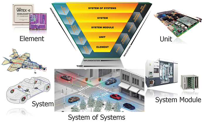
Systems design methodology is often illustrated with the V Diagram (FIGURE 1). The V Diagram graphically shows how a typical system is designed, from concept through first product shipment. The process begins with the decomposition stage, beginning with a system-of-systems. For example, the first definition in the decomposition stage might be “we’re going to design a communications satellite.” That’s an exceptionally broad definition, but it is how just about every project begins. Decomposition continues until the individual circuit elements are defined by the circuit designer. The right side of the V begins the implementation of the project, in the reverse order from element to system-of-systems.

Figure 1. Systems design is often illustrated with the V Diagram, describing the design decomposition process, followed by the implementation process that every product encounters.
From the perspective of PCB design, the PCBs become modules within a system. Thus, the PCB design should begin with a logical representation of the PCBs. Then, the required interconnections between the boards can be defined.
Other criteria as well must be considered when partitioning the functions into logical PCB representations. For example, it is likely the thermal dissipation needs to be relatively evenly distributed across the physical PCBs. For some systems, weight is a primary constraint, or weight and weight distribution across the system are paramount. High-speed design requirements may constrain certain parts to reside on the same PCB to ensure signal integrity.
In each of these cases, and many more, rearranging the location of functions among logical PCBs and reconfiguring the interconnections may occur multiple times before the design is frozen. With current methods, this could mean substantial manual effort, and substantial opportunity for errors.
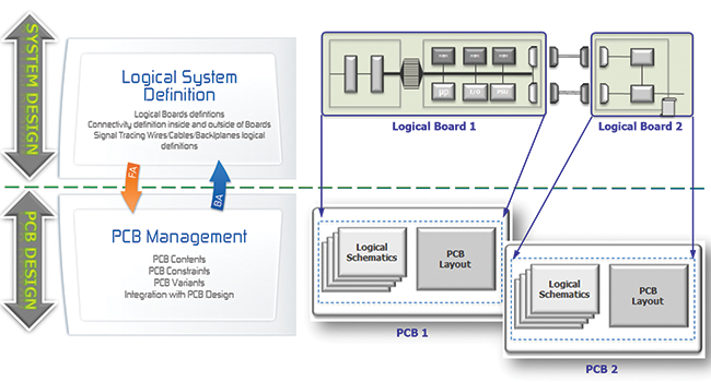
And, let’s not forget that changes to the system design are not limited to the logical PCB stage. Problems can, and do, creep up at all stages of the design flow and sometimes require re-partitioning of the functions among the boards; thus communication between the systems designers and PCB designers must take place to implement the changes (FIGURE 2).

Figure 2. As changes to the design occur, rapid and accurate communication must take place between the systems designers and the PCB designers.
Connector Management
We’ve already defined many of the potential trouble areas in a system design, but the magnitude of one of those problems is sometimes overlooked: connector management. While it is certainly not trivial to redesign several PCBs because a thermal problem required moving circuit elements around to other locations, the sheer number and constraints associated with connections between the boards is astounding. The inevitable changes will cause anyone to take notice when they have to move those connections without errors.
Moving the signals from one connector to another is a task that will cause most people’s eyes to cross. But that’s just part of the task. Some of those signals will be constrained because of speed concerns. Others might be constrained by length or by current carrying capacity. All these constraints must be cataloged and applied when a change takes place.
Clearly, the number of connections of high-end systems, coupled with the extended set of constraints, has made connector management just about beyond the capability of any human being. So, what kind of automation is needed to manage systems connections so that all are done accurately and all constraints are applied?
Systems Design Automation
A systems design platform should incorporate a drawing tool so that the designer can quickly produce logical systems diagrams and interconnections. Automation should track each interconnection and ensure all constraints are maintained. Changes should be not only quick and accurate, but easily communicated to other project groups and should synchronize the design.
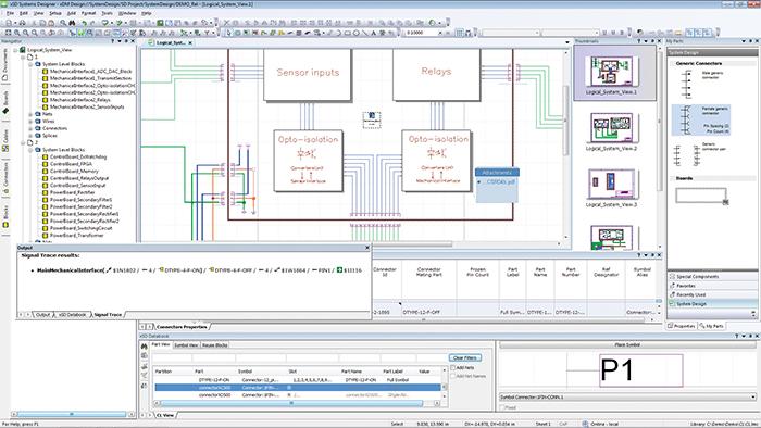
Systems design automation products are being developed that achieve these goals and allow quicker, more accurate designs that can be readily (and accurately) modified during the design process. With the drawing tools, the systems designer can define the functionality and interconnection among the individual boards in the system (FIGURE 3). The automation tracks every function, interconnection and constraint.

Figure 3. Automation tools allow the systems designer to place functions on individual logical boards and to define the logical interconnection among the boards.
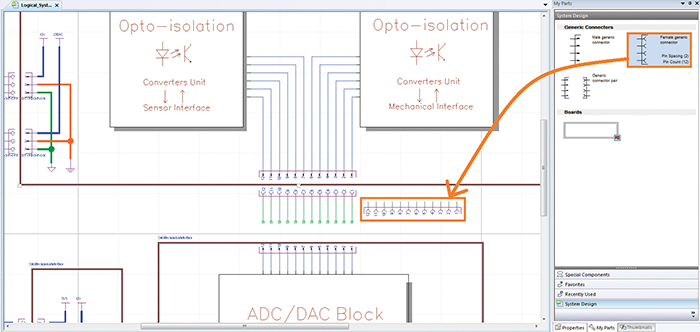
As system design evolves, the logical and physical designs are synchronized, providing users with an accurate system representation (FIGURE 4). When changes ultimately arrive, the design automation allows the systems designer to add or change connectors (FIGURE 5), and as logical elements are moved among the boards, the connectivity moves right along with them. Once a change is made, the design automation ensures that the new configuration is communicated to other teams and that the design is synchronized.

Figure 4. The entire logical system is represented, and automation tracks functions assigned to logical boards, as well as the interconnections.

Figure 5. Changing a connector becomes a matter of dragging the new connector type to replace the existing one. All signals are mapped and connected correctly, by design.
Summary
More products are entering complex systems design, combining multiple PCBs into a single system, which may then become part of a system-of-systems.
Current methodology inserts unnecessary costs, in both time and money, into new product design. Errors cost time, money and lost opportunity. Failure to maintain the integrity of even a single interconnection could result in delay, thousands of dollars to resolve and perhaps even an expensive product recall. To combat these possibilities, some manufacturers have built-in “fail-safe” precautions, but these too add cost to every unit.
This increasing complexity has just about placed managing the functions and interconnections of the system outside of the capabilities of humans. What is needed at the multi-board system level is a similar revolution to provide a solution that automates the enormous connection management problem, facilitates easy system and logical design and integrates seamlessly with the PCB design flow. Such products will turn a tedious, often error-rich procedure into a smooth and quick process that eliminates human errors.
Rainer Asfalg is product line director and Andy Watts is product marketing manager at Mentor Graphics (mentor.com); This email address is being protected from spambots. You need JavaScript enabled to view it..


