The parameters of ESO, and how to efficiently ensure a design will pass.
Most readers are familiar with the release of a PCB design to manufacturing, and the associated “signoff” that the design data must pass. This manufacturing signoff ensures that the production rules are abided by so that the board can be fabricated without error, at sufficient yield, and meets other manufacturing criteria.
With the increasing complexity and speed of current designs, along with the availability of simulation and analysis tools, many companies are instituting procedures for electrical signoff, or ESO. This procedure subjects the design to rigorous rules to ensure that system timing, signal integrity, power integrity and EMI/EMC are all within established limits.
What constitutes the parameters of ESO, and how to most efficiently ensure a design will pass? And what steps must be taken for a design pass the first time, without the expense of reworking the design?
Electrical Signoff
The ESO process is a set of checks that verify a design meets all specifications before it can be sent to manufacturing. The ESO terminology has been used within most IC design flows for the final verification steps. In recent years it has been applied to PCB design flows as well. Here, the focus is on “electrical rule signoff.” ESO basically means that a design meets all electrical performance objectives.
The design complexities introduced by higher routing densities and widespread usage of ICs with fast-edge rates make it quite challenging to exhaustively verify a PCB design’s electrical performance. Being a new process in the PCB design world, few companies have set up procedures in their design methods and ESO procedures to ensure passing the first time. Some companies still accept that it will take multiple spins to get the design passed to manufacturing for prototypes. This approach is known to be expensive, sacrifices precious time to volume (and profits), and many times delivers a product with unknown quality that could lead to higher field failure rates.
Available simulation and analysis tools have made modeling, finding problems, resolving the problems, and ultimately passing ESO much more automated, comprehensive and thorough. These tools come preloaded with design rules for checking designs before, during, and after layout. In addition, companies can design their own rules for specific parameters on the design.
Another advantage is that automated rule checking covers the complete design. With manual checking, and the unavailability of time to check every net, decisions are made as to which are “critical nets.” Unfortunately, there are countless stories of thorough verification of critical nets only to have a major problem develop on prototypes, or worse, in the field.
ESO Methodology
Let’s look at an example PCB design and develop an ESO methodology. First, a comprehensive set of rules needs to be developed (or the built-in rules need to be parameterized). FIGURE 1 shows a set of rules for this example. These rules cover all the ESO parameters mentioned earlier: SI, PI, EMI/EMC, timing, differential pair impedance, decoupling capacitors, and various layout rules.
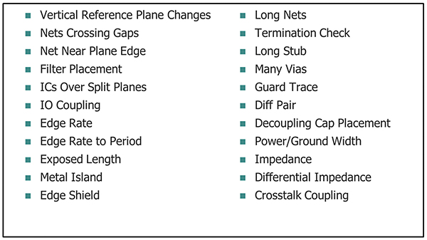
Figure 1. An example rule set that will verify required ESO parameters.
The ESO methodology in our example starts early in the design flow as performance-sensitive nets are identified as part of rule parameterization. FIGURE 2 shows an ESO methodology, and is differentiated for high-density boards, high-speed boards, and “others.” Of course, many high-speed boards are also high density, so the two paths can be combined.
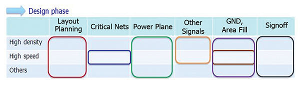
Figure 2. Rule sets for the ESO methodology in this example.
Layout planning. Even during pre-layout floor planning, simulation can help clearly define layout constraints and PCB layer stackup. This helps reduce the amount of layout rework required as more of the layout topology solidifies. Using simulation to find potential electrical performance design flaws during layout creation enables the layout team to iterate immediately, when it is least expensive. Violations are identified, as in FIGURE 3. Each violation can be systematically resolved, which may require further layout repair and iteration until desired electrical performance is achieved. Then the design can move with a clean foundation. As the layout progresses, additional checks can be performed as shown in FIGURE 4.
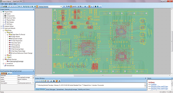
Figure 3. As the floor planning progresses, initial rule checks can begin. Eliminating flaws at this stage is quick and costs nothing.
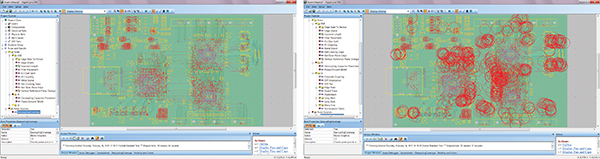
Figure 4. As the layout progresses, more rules can be checked. While still in simulation, even at late stages in the layout, corrections are relatively quick and inexpensive to fix.
Critical nets. Simulation of critical nets is one of the most important tasks to ensure ESO. Timing problems, differential pair impedance and signal integrity are all concerns for these nets. Simulation can be run both pre- and post-layout. During pre-layout design, rules help engineers set the appropriate parameters. Design parameter sweeps help designers better tune drivers, interconnect and termination constraints by ensuring the entire available design space has been explored. During and after layout, signal integrity can be checked.
For example, when designing a DDR memory layout, the rule check tools can automatically extract the layout interconnect, perform the thousands of timing path simulations that account for crosstalk, and generate comprehensive reports and waveforms for data/strobe, strobe/clock, addr/amd/dtrl, and other setup and hold times. Timing failures are easily identified and flagged as pass or fail. Deeper simulation may be in order at this point to better quantify the failing design violation’s degree of severity (FIGURE 5). DDR timing and electrical signoff can be achieved only when these timing failures are resolved.
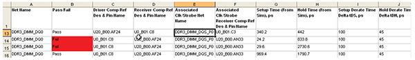
Figure 5. The complete timing analysis allows timing failure to be easily identified, allowing correction before hardware is built.
Power plane, ground, area fills. Despite the seeming simplicity, the power plane is a significant part of any PCB design, especially high-speed designs. Also, high-density designs often require the power plane to conform to less-than-optimum shapes, which can induce problems. Analysis must be done for both AC and DC.
As part of the pre-layout design process, DC drop analysis helps guide the designer toward general power plane shapes, ensuring adequate copper weighting to meet expected current requirements. DC drop analysis identifies high-current flow regions and allows layout adjustments to “spread out” the current demand. Voltage rails with excessive voltage drop, vias with high current, and other areas of the layout with excessive current density can cause problems … often not manifesting themselves until thermal degradation causes a field failure.
Power planes must be able to supply enough current to maintain the supply voltage at every power pin on every IC, within tolerance. DC drop analysis can determine the plane voltage and current density at every point, ensuring that any out-of-tolerance area can be fixed.
Fast edge-rate ICs have created design challenges for PCB power distribution networks (PDN). Since transient current must be supplied to these fast-edge-rate drivers for proper operations, managing the impedance between the power and reference plane is critical for ensuring PDN can supply current quickly when needed. To meet ESO, sources of AC noise minimization of the impedance of the PDN are required. As seen in FIGURE 6, this noise and current-transient spikes can cause quite a ruckus on the power plane!
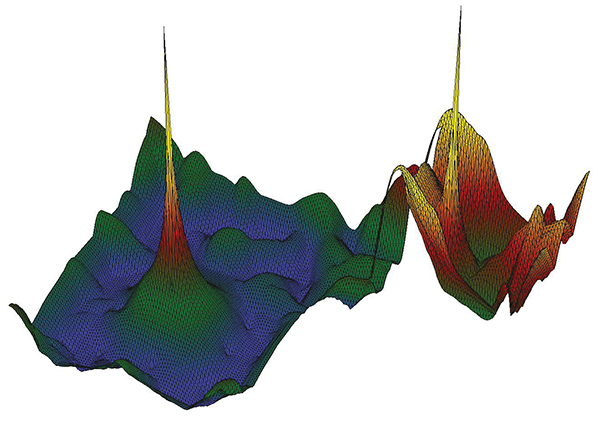
Figure 6 This plot of noise on the power plane of a PCB design shows that noise can cause unwanted transients, PI problems, and also generate EMI.
Other signals. All critical signals should be checked for signal integrity (SI) during and after the completion of the layout. For example, each SerDes channel can be analyzed with its characteristic eye diagram and bit error rate (BER). If necessary, specific layout sections, such as BGA breakouts or traces through a pin-field must be modeled with more accuracy. Final channel eye quality assessment (good eye mask) and BER can be used as key electrical signoff metrics for SerDes channels.
Simulation is also used to identify timing violations for all nets. The simulation results should show timing path characterization, with all crosstalk and other signal coupling effects considered. Violations are identified and need to be resolved in order to reach electrical signoff.
Signoff! At this point, the layout is complete. The pre-layout analysis and simulation has led to the optimal stackup and placement of components. Simulation during the layout identified and allowed flaws to be fixed … before hardware was built. Finally, post-layout simulation accounted for the entire design and discovered any latent problems that could be fixed before ESO.
A systematic electrical signoff process for high-speed PCB design has been presented here. Performing electrical signoff tasks as a natural part of the circuit design and layout process will be become increasingly common.
Rod Dudzinski and Minoru Ishikawa are market development managers. System Design Division at Mentor Graphics; This email address is being protected from spambots. You need JavaScript enabled to view it..


