Or why parts should be “implemented,” not just “installed.”
By and large, PCB assembly up to now has been rather traditional. Surface mount technology has made significant inroads to account for the greater majority of assembly technology compared to through-hole.
However, these days PCB assembly takes on new levels of technology, complexity and service requirements differently. At level one, OEMs require standard assemblies based on standard, defined processes and expect 100% yields, or close to them.
At level two, challenges are involved, but the technology and OEM expectations are defined, and yields are relatively high. Generally, the OEM customer conveys their expectations in terms of the latest IPC revision, functionality and performance. With that information, the EMS provider moves on to develop the process and fulfill the OEM’s requirements.
A new “level three” is beginning to be recognized on the assembly floor. In this case, the OEM customer’s expectations aren’t very defined, even to themselves. Under typical circumstances, a design is not known to be successful until a working prototype is built. For the contract manufacturer, it is imperative to understand those OEM expectations, and to determine ways to handle the project and use a package “implementation” approach, rather than package “installation” approach, to comply with those requirements.
What defines this third level of assembly? PCB assemblies that can best be characterized as changing and evolving and becoming extensively complex in terms of packages used; high frequency (above 5GHz); the assembly requirements, and of course, customer expectations. For instance, a third-level assembly would be a digital board with a high-density, extremely populated landscape, or a highly integrated, double-sided, fully populated board with µBGAs, DSPs, LGAs, digital wafer-level packages, and miniatures such as 01005 passives.
This third level harbors a considerable number of gray areas, such as the process option for high-density digital population, which could be very different than that needed for a microwave/RF assembly. The tooling and processes for a successful prototype build will vary accordingly.
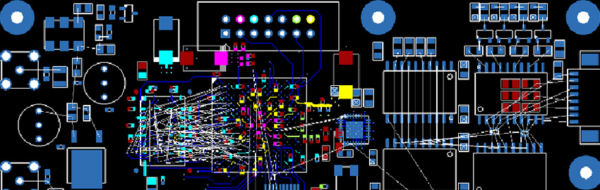
High-frequency digital, microwave and RF assemblies closely match this third level of assembly insofar as the similarity of challenges (Figure 1). The commonality is that the EMS provider and OEM must develop a comprehensive approach to fabrication and design for manufacturing (DfM), design for assembly (DfA), and design for test (DfT) for producing the prototype, and be conscious of customer expectations versus assembly requirements. Moreover, each of those assembly areas demands greater depth in terms of meeting the demands of a particular third-level PCB assembly project.
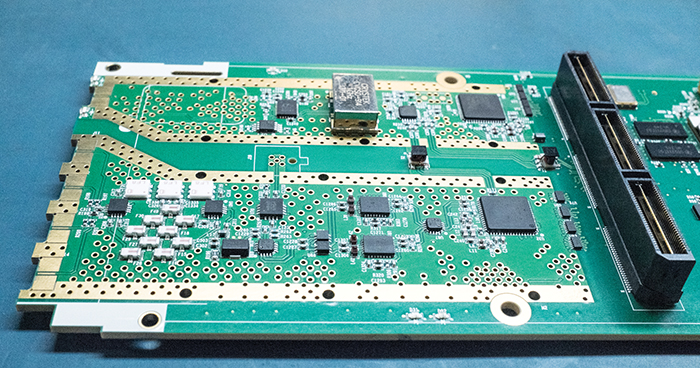
Figure 1. An RF PCB assembly.
Design verifications, performance optimizations, noise and EMI issues play critical roles. They are important because the OEM is advancing a design that is not verified or confirmed. Often, the OEM may not have experience with the critical aspects of process definition and development, and type of verification needed before money and effort is invested to move the assembly to the prototype or first-article inspection (FAI) level. This calls for a comprehensive approach dealing with the design of experiments and both levels of package implementation and assembly process development for prototype runs.
In the case of high-speed assemblies, it is important to confirm whether the PCB is in compliance with the OEM requirements (fabrication DfM). Sometimes it’s necessary to perform some kind of testing at the bare-board level to determine any signal integrity, leakage or performance issues. Above 750MHz, assembly performance can drastically change, unless the following issues are addressed:
- Pre-assembly PCB testing against impedance and point-to-point.
- Run DfM during the layout stage on bill of materials (BoM) and all critical parts’ footprints.
- Compare the assembly process requirements against the different packages of LGAs, DSP, RF filters, PoP (package-on-package), fine-pitch BGAs and all low-profile packages.
- Choice of solder paste: water-wash or no-clean. If no-clean, does flux residue need to be cleaned at a later assembly stage?

Keep in mind that this list represents a sampling; there are others.
It’s important to note that in any electronics assembly, signal generation, transfer, processing, strength, and noise management are key factors to optimize circuit performance. At this stage the OEM is not quite sure what to expect, unless the first few units are successfully produced and tested, and a comprehensive design-of-experiments of the prototype assembly process has been developed.
‘Implement, don’t install.’ A key part of the prototype assembly process is developing a process where LGAs, µBGAs, high-count BGAs, die-scale packages or DSPs, PoP and RF filters and packages can be properly implemented without losing performance, minimizing noise, and correctly handling heat transfer issues. That’s why it is vital to implement the packages rather than install them (Figure 2). At the same time, it’s vital to check and reduce the gray areas. Those gray areas may present problems unforeseen to OEMs or EMS providers.
Figure 2. A close-up of an LGA package implemented on a PCB.
There are two major differences between implementation and installation. When a package is implemented, the user knows precisely what is expected of it, the frequency levels at which the package will operate, the kind of fatigue the package will endure in terms of vibration and heat cycles, and so on.
Also, when packages are implemented, other considerations include choosing the right solder paste, developing the solder paste stencil and a robust SMT reflow profile, choosing the right pick-and-place line, and developing the proper process for flux residue removal.
Any flux residue under the packages or on the PCB can shift the performance of the packages and can lead to the total failure of the assembly. Each step is very important for a successful first article/prototype run, leading to a production run with high yield.
For example, any heat transfer must be properly managed, such as heat, solder, and solder flux residue under the LGAs and low-profile packages. In the case of LGAs, if the packages lack solder bumps, the solder joint formed could be marginal, unless proper stencil design is implemented. PCB or package warpage or solder fluxes left over from the process can lead to improper performance assembly and lower yield.
High yield considerations. When the requirement is 100% yield or close to it, every device package needs extra attention during PCB design and process development. In particular, this includes µBGAs, BGAs, DSP (die-scale packages), LGAs, PoP, and other packages.
Steps to take include ensuring an even distribution of copper as much as possible along the landscape of the package. Pad size should be non-solder-mask-defined (NSMD) for BGA, µBGAs, and any other packages that generate extra heat. The NSDM pads are more thermal-fatigue-resistant.
Detailed x-ray per IPC-7095 plays a valuable role in identifying assembly defects. Voids need to be considered as well. A certain percentage of voids in BGA solder joints can change a package’s performance. IPC standards allow 25% voids in all types of solder joints. But in the case of a high-speed assembly, a determination needs to be made on what percentage of voids is permissible. Endoscopic inspection is essential, as well, and should be performed close to the BGA balls to determine and verify the type of ball collapse (Figure 3) and package warpage.
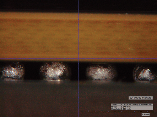
Figure 3. Proper ball collapse on a BGA assembly.
High-pin-count BGAs also have their own gray areas. For example, to compensate against head-in-pillow (HiP) defects, one approach is to include a little extra copper on the outer pads. For µBGAs and CSP packages during assembly and when performing thermal profiling, place at least three to four thermocouples covering all BGAs to determine that temperature variation is not more than 5⁰C. Also, time above liquids (TAL) should be even throughout the BGA package when it is entering the cooling cycle. Otherwise, a reflow fixture could be required to avoid HiP defects (Figure 4).
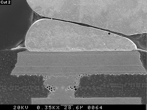
Figure 4. SEM photo of a head-in-pillow defect.
The die-scale package poses gray areas as well. This package has been around the assembly floor for some time, and it presents different challenges. In this case, the entire die or chip is implemented without a heat sink. This calls for a heavy thermal transformer from the package to grounding, lest the package burn out. So, the challenges are at the grounding level.
Then there are the undefined areas of the project. These occur when an OEM isn’t quite sure of some critical parameters, packaging, or design questions. Also, for assemblies featuring higher than 750MHz frequencies, solder paste choice, secondary cleaning (if required), critical solder paste volume, and voids and their effects on assembly performance, must be taken into account.
While IPC standards permit 25% voids in solder joints, even in Class 3 assemblies, in high-frequency circuitry voids can cause noise and signal damping and change the performance of an assembly. PCB surface plating can contribute to voids in solder joints as well.
In cases like this, to balance out these OEM uncertainties, the EMS provider must develop a comprehensive process. All processes and assumptions must be based on previous experience and so-called “tribal knowledge.” For the EMS provider to resolve the issues presented by the OEM, it must apply these major steps:
- Comprehensive assembly process development.
- Run successful first article inspection (FAI).
- Support customer in testing (flying probe or ICT).
- Provide any upgrades needed to the assembly process.
- Develop the NPI in extreme detail.
- Provide detailed step-by-step work instructions as defined by the customer.
For the OEM these steps can represent unchartered waters, but it cannot be that way for the EMS provider. Otherwise, by not applying the necessary knowhow and experience, the OEM customer will incur larger than expected cost.
It is well-known in electronics manufacturing that FAI and the prototypes prove a design, and running the first units through assembly provides the results that define OEM customer expectations. Up to that stage, the OEM won’t be sure of what to expect from that assembly. If that particular assembly isn’t performed and executed properly, then the undesired results will serve as the basis for the OEM’s expectations.
Therefore, it is up to the EMS provider to take the lead and help the OEM better define their expectations. That can be accomplished by enriching performance by selecting a highly robust process to minimize noise and leakages, as well as maintaining good signal integrity, among other major improvements. At this prototype stage, the OEM will be in a position to define their expectations.
Mueed Khan is director of manufacturing at NexLogic Technologies (nexlogic.com); This email address is being protected from spambots. You need JavaScript enabled to view it..